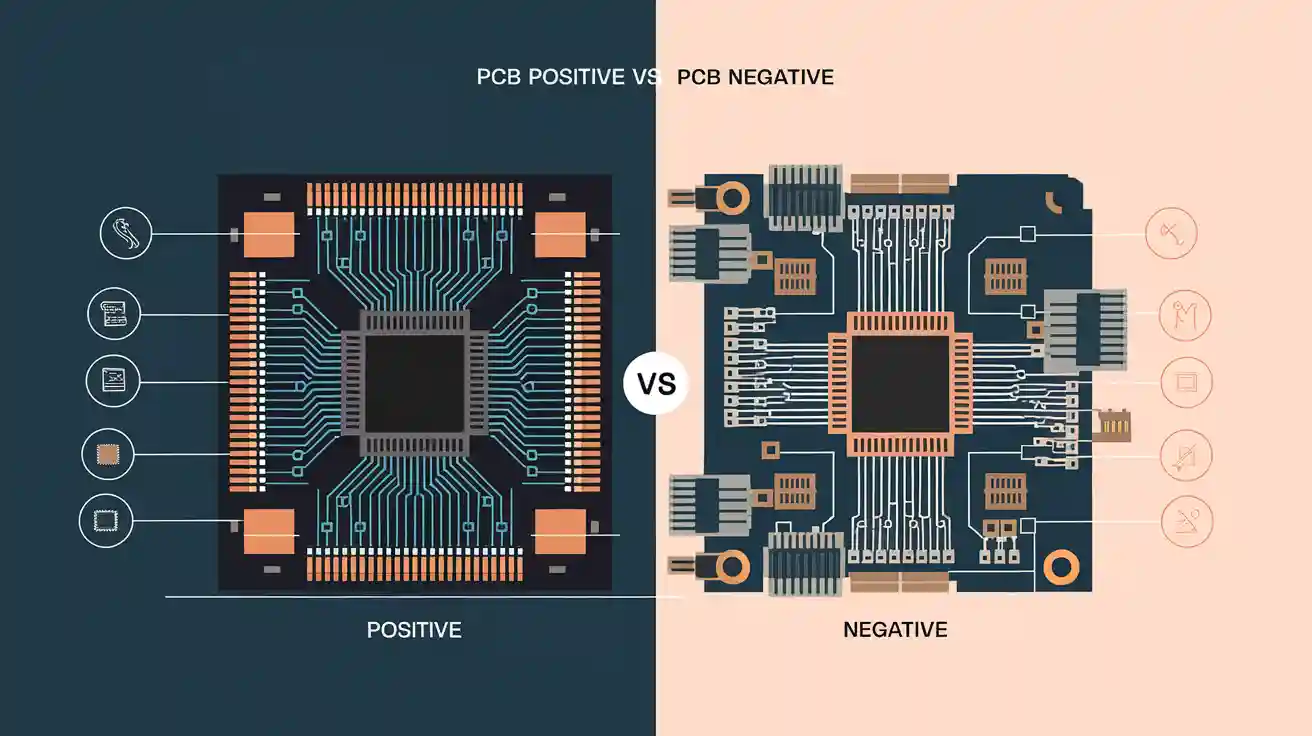
Understanding PCB Positive and Negative Methods
Explore the key differences between PCB Positive and Negative.
Features | PCB Positive | PCB Negative |
|---|---|---|
Protected Area | Circuit traces | Spaces between traces |
Photoresist Covers | Areas to keep | Areas to remove |
Result After Etching | Traces remain | Spaces remain |
Common Use | Simple or single-layer boards | Complex or multi-layer boards |
Production Time | Usually shorter | May take longer for complex boards |
Copper Plane Control | Basic | Advanced |
Best For | Simple boards | Complex boards |
Layout Style | Matches final copper | Inverse of final copper |
You may ask how PCB Positive and PCB Negative are different. PCB Positive keeps the parts you want safe, and takes away the extra copper. PCB Negative works in the opposite way. Each way has its own steps and is used for different jobs. You pick one based on what your project needs and what you want to make.
Definitions
PCB Positive
You use PCB Positive to keep the copper that forms the circuit. First, you put photoresist on the parts you want to save. Light is used to make the photoresist hard on those parts. Next, you take away the extra copper. Only the circuit pattern stays. This way, you can see the copper traces as they will look on the board.
PCB Negative
You use PCB Negative to keep the spaces between the circuit paths safe. Here, the photoresist goes on the parts you do not want to keep. Light makes the photoresist hard on the spaces between the traces. Then, you remove copper from the parts that are not covered. This leaves the spaces empty and the traces are still there.
Tip:
You can use the table below to quickly see the main differences between PCB Positive and PCB Negative.
Feature | PCB Positive | PCB Negative |
|---|---|---|
Protected Area | Circuit traces | Spaces between traces |
Photoresist Covers | Areas to keep | Areas to remove |
Result After Etching | Traces remain | Spaces remain |
Common Use | Simple or single-layer boards | Complex or multi-layer boards |
How It Works
Film and Photoresist
You start both PCB Positive and PCB Negative processes with a thin film called photoresist. This film reacts to light. In PCB Positive, you cover the copper board with photoresist. You place a film with your circuit design on top. The clear parts of the film match the traces you want to keep. Light passes through these clear areas and hardens the photoresist below. The dark parts block the light, so the photoresist stays soft there.
In PCB Negative, you also use a photoresist layer. This time, the film has dark areas where you want to keep copper. Light hardens the photoresist only in the spaces between the traces. The traces themselves stay covered by soft photoresist. This difference in film design changes which parts of the board get protected.
Note:
The way you use the film and photoresist decides which parts of the copper board stay and which parts go.
Exposure and Etching
After you set up the film and photoresist, you move to the exposure step. You shine light onto the board. In PCB Positive, the light hardens the photoresist on the traces. You wash away the soft photoresist, which leaves the copper traces covered and the rest exposed. Next, you use a chemical to etch away the exposed copper. Only the traces remain.
With PCB Negative, the light hardens the photoresist in the spaces between the traces. You remove the soft photoresist from the trace areas. When you etch, the chemical removes copper from the traces, not the spaces. The result is the opposite pattern compared to PCB Positive.
You can see that both methods use light and chemicals, but the way you protect the copper changes the final board.
Design Differences

Positive vs Negative Planes
You will notice a big difference when you look at the planes in PCB Positive and PCB Negative designs. In PCB Positive, you see copper traces and pads as the main features. The design shows the parts you want to keep. You protect these areas during the process. This method works well for simple boards, where you need clear and easy-to-follow paths.
In PCB Negative, you focus on the spaces around the traces. The design highlights the areas you want to remove. You protect the gaps and let the traces get etched away. This approach helps when you work with complex boards or need tight spacing. You can use negative planes to create ground or power layers with fewer breaks.
Tip:
If you want to keep your design simple, choose PCB Positive. If you need more control over large copper areas, try the negative method.
Layout Representation
You can see the difference in layout when you compare the two methods. In PCB Positive, the layout matches the final copper pattern. You see the traces, pads, and shapes as they will appear on the finished board. You can check your design and spot mistakes easily.
In PCB Negative, the layout looks like a photo negative. The spaces between the traces stand out. You may find it harder to read at first, but this style helps when you design multi-layer boards. You can use negative layouts to create solid planes for power or ground. This makes your board stronger and reduces noise.
Here is a simple table to help you compare:
Feature | PCB Positive Layout | PCB Negative Layout |
|---|---|---|
Main Focus | Traces and pads | Spaces between traces |
Visual Style | Matches final copper | Inverse of final copper |
Best Use | Simple, clear designs | Complex, multi-layer |
You can use both layout styles in design software. Try each one to see which fits your project best.
Process Steps
PCB Positive Process
First, you clean the copper board. This gets rid of dust and oil. Next, you put photoresist on the board. You use a clear film with your circuit design. The clear parts show the traces you want to keep.
You shine UV light on the board. The light makes the photoresist hard under the clear spots. The photoresist under dark spots stays soft. You wash the board with a developer. This takes off the soft photoresist. The hard photoresist stays on the traces.
Now, you start etching. You dip the board in an etching solution. The solution takes away the copper that is not protected. The copper under the hard photoresist does not get removed. After etching, you clean off the last photoresist. Only the copper traces for your circuit are left.
Tip:
The PCB Positive process is good for simple designs. You can see the traces like they will look on the finished board.
Typical Steps in PCB Positive:
Put on photoresist.
Place the positive film.
Shine UV light.
Develop the board.
Etch away extra copper.
Remove the photoresist.
PCB Negative Process
You start the PCB Negative process the same way. Clean the copper board and add photoresist. This time, you use a negative film. The dark parts match the traces you want to keep.
You shine UV light on the board. The light makes the photoresist hard in the spaces between traces. The photoresist under the dark parts stays soft. You develop the board to take off the soft photoresist from the trace areas.
Next, you etch the board. The etching solution takes away copper from the traces. The hard photoresist keeps the spaces between traces safe. After etching, you remove the last photoresist. The traces are left with open spaces around them.
Note:
The PCB Negative process is helpful for solid copper planes or multi-layer boards.
Typical Steps in PCB Negative:
Clean the copper board.
Put on photoresist.
Place the negative film.
Shine UV light.
Develop the board.
Etch copper from traces.
Remove the photoresist.
Comparison Table: PCB Positive vs PCB Negative Process
Step | PCB Positive Process | PCB Negative Process |
|---|---|---|
Film Type | Positive (clear traces) | Negative (dark traces) |
Protected Area | Traces and pads | Spaces between traces |
Etching Removes | Unwanted copper | Copper from trace areas |
Best For | Simple, single-layer boards | Complex, multi-layer boards |
Production Time | Usually shorter | May take longer for complex boards |
🛠️ Quick Fact:
You can finish a PCB Positive board faster for easy projects. PCB Negative takes more time, but works better for hard designs.
Pros and Cons
PCB Positive Advantages
There are many good things about using PCB Positive.
You can easily see your circuit traces while you work.
This method is great for simple and single-layer boards.
You can finish making your board quickly because the steps are easy.
You might spend less money on small projects or test boards.
Tip:
PCB Positive lets you find mistakes early. This can help you save time and money.
PCB Positive Disadvantages
There are some problems with this method.
It does not work well for complex or multi-layer boards.
You do not get much control over big copper areas or ground planes.
The process gets harder if your design is large or has lots of details.
PCB Negative Advantages
PCB Negative has strong benefits for advanced designs.
You can make solid copper planes for power or ground layers.
This method is good for complex and multi-layer boards with tight spaces.
You get more control over big copper areas. This can make your board stronger and lower electrical noise.
Feature | PCB Positive | PCB Negative |
|---|---|---|
Best for | Simple boards | Complex boards |
Copper plane control | Basic | Advanced |
Multi-layer support | Limited | Excellent |
PCB Negative Disadvantages
There are some hard parts with PCB Negative.
The process can take more time, especially for boards with lots of details.
The layout may be hard to read when you first start.
Making small numbers or simple boards can cost more money.
Note:
Pick the method that fits your project best. Each one works better for different jobs.
Applications
When to Use PCB Positive
Pick PCB Positive if you want a quick and easy process. This method is best for single-layer or double-layer boards. It is good for making prototypes or small batches. You can see the circuit traces well, so you can check for mistakes before you finish.
Many students and hobbyists use PCB Positive for school work or fast tests. This method is also good if your design has wide traces and does not need tricky copper planes. If you want to save time and money, this method is a smart choice.
Tip:
Choose PCB Positive for simple layouts, easy circuits, and when you need to fix things fast.
Trying out new ideas and testing
School or learning projects
Basic electronics for home use
Fixing boards or making spare parts
When to Use PCB Negative
Use PCB Negative if your project needs more features. This method works well for multi-layer boards or designs with small spaces. If you need solid copper planes for power or ground, PCB Negative gives you better control. You can make hard layouts with lots of connections and tiny gaps.
Engineers use PCB Negative for fast circuits or devices that need strong power. This method helps lower electrical noise and makes the board stronger. If you work on pro products or big jobs, you will like how exact this process is.
Note:
Pick PCB Negative for hard layouts, multi-layer boards, and when you need strong copper planes.
Advanced electronics and machines
Multi-layer PCBs
Circuits that need high speed or power
Boards with lots of parts close together
Application Type | PCB Positive | PCB Negative |
|---|---|---|
Prototyping | ✅ | |
Simple Circuits | ✅ | |
Multi-layer Boards | ✅ | |
Power/Ground Planes | ✅ | |
High-Speed Circuits | ✅ |
Choosing the Right Method
Key Factors
When you pick between PCB Positive and PCB Negative, you should think about a few important things. Each method is best for certain projects. You want your choice to fit your design, your budget, and how many boards you need.
Here are some key points to help you decide:
Board Complexity
If your board is simple and has one or two layers, PCB Positive is quick and easy. You can see your circuit as it will look when finished. If your board is complex with many layers or small spaces, PCB Negative gives you more control and helps with hard designs.Copper Plane Needs
Sometimes you need big copper areas for power or ground. PCB Negative lets you make solid planes with fewer gaps. This is good for fast circuits and helps lower electrical noise. PCB Positive is fine for basic boards but does not give much control over large copper areas.Production Volume
If you only need a few boards or are testing ideas, PCB Positive saves time and money. You can fix mistakes fast. If you want to make lots of boards or need them to be very reliable, PCB Negative is better for big jobs and pro products.Design Software Compatibility
Most design programs work with both methods. Check if your software lets you switch between positive and negative layouts easily. This can help you save time when you design and build your board.
Tip:
Always think about your project goals before you pick a method. Ask yourself how hard your board is, how many you need, and what features are most important.
Factor | PCB Positive | PCB Negative |
|---|---|---|
Best for | Simple, quick boards | Complex, multi-layer |
Copper plane control | Basic | Advanced |
Production speed | Fast | Moderate |
Cost for small runs | Lower | Higher |
You can use this table to compare what you need. Choose the method that fits your project to get the best results.
You have learned how PCB Positive and PCB Negative are not the same. PCB Positive is good for easy and fast projects. PCB Negative is better for hard or multi-layer boards. Look at this table to help you pick:
Your Need | Best Choice |
|---|---|
Simple design | PCB Positive |
Complex layout | PCB Negative |
Make sure you pick the right method for your project. Ask your manufacturer for help if you are not sure.
FAQ
What is the main difference between PCB Positive and PCB Negative?
PCB Positive keeps the traces safe. PCB Negative keeps the spaces between traces safe. PCB Positive is best for easy boards. PCB Negative is better for hard or multi-layer boards.
Which method is faster for making a PCB?
PCB Positive is usually quicker to finish. The steps are simple and easy. PCB Negative takes longer, especially for tricky or layered boards.
Can I use both methods for any PCB design?
Both methods work for many board types. PCB Positive is good for simple, single-layer boards. PCB Negative is better for hard layouts or when you need big copper planes.
Which method gives better control over copper planes?
PCB Negative lets you control big copper areas better. You can make strong power or ground planes. PCB Positive only gives basic control, which is fine for easy circuits.
Is one method cheaper than the other?
PCB Positive usually costs less for small jobs or tests. PCB Negative can cost more, especially for hard or big jobs.