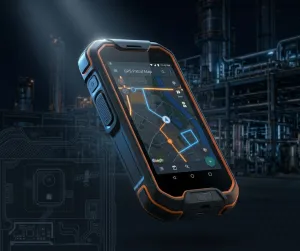
Smart Inspection Device Case Study: Designing a GPS-Enabled, Camera-Integrated Industrial Patrol Terminal
1. Project Overview 1.1 Client Background The client runs a security systems integration and industrial services business. Their customers span property management companies, utility operators, oil and gas facilities, and large manufacturing plants. These are not small sites. Some of them cover hundreds of acres. Some run 24-hour operations where a missed patrol checkpoint at 3 AM is not a paperwork problem. It is a liability. For years, their patrol staff carried RFID wands, tapping checkpoint cards at fixed locations, then filing paper logs at the end of a shift. The system proved one thing: a guard reached a specific spot at a specific time. Everything else, what they saw, what condition the equipment was in, whether anything unusual happened between checkpoints, none of that was captured. So the client came looking for smart inspection device. 1.2 Project Objectives The smart inspection device needed to do several things simultaneously and
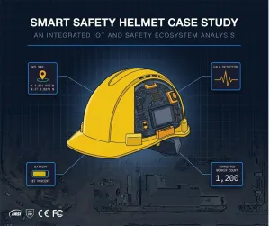
Smart Safety Helmet Case Study: Designing an IoT-Enabled Industrial Protection Helmet
1. Project Overview 1.1 Client Background The client runs an industrial smart safety helmet selling into construction, mining, oil and gas, and heavy manufacturing. They held passive PPE certifications and had a solid dealer network across three continents. The problem was competitors were shipping connected helmets, and this company had nothing to answer with. The brief was to take a certified hard hat shell and turn it into a live IoT device, without losing EN 397 and ANSI Z89.1 ratings in the process. Also read: Smart Early Education Learning Tablet Case Study 1.2 Project Objectives We focused on the Six deliverables from day one. Every engineering decision downstream answered to these six requirements. 2. Industry Challenges in Smart Helmet Development 2.1 Harsh Industrial Environments Construction sites run heavy plant machinery that generates constant vibration. Mining tunnels combine high humidity with fine dust. Offshore platforms add salt spray and shock events

Smart Early Education Learning Tablet Case Study: Designing an AI-Powered Interactive Learning Device for Children
Case Study: OEM / Hardware Engineering Smart Early Education Learning Tablet Designing an AI-Powered Interactive Learning Device for Children Industry EdTech Hardware Markets North America, Europe, SEA Device Type AI Kids Learning Tablet 1. Project Overview 1.1 Client Background An education technology brand walks into smart early education learning tablet development. Sounds like the start of a joke, but it is actually one of the more interesting pivots happening in edtech right now. This client had built a real presence in mobile app learning, preschool and early primary markets, with solid user traction across North America, Europe, and Southeast Asia. The apps worked. Parents downloaded them. Kids used them. But here is the problem nobody talks about openly: a shared family phone is a terrible learning environment. The child drifts. Notifications pull attention. Older siblings have different apps installed. Parents hand over a device and then spend the next twenty

AI Translator Device Case Study: Designing a Real-Time Multilingual Smart Translation System
Building a real-time voice translator demands intense edge computing and flawless acoustic design. This case study details the engineering behind a multilingual ai translator. You will explore hardware architecture, neural machine translation hardware, and the strict demands of an AI translation device manufacturer. The goal is mastering seamless, instantaneous cross-cultural communication hardware. 1. Project Overview 1.1 Client Background First, you need to understand the exact motivation of the client. A major consumer electronics brand wanted to build an AI translator device to capture the surging post-pandemic travel boom. Target markets explicitly included international travelers navigating foreign transit systems, business users negotiating complex deals, and cross-border e-commerce professionals. Also Read: Automotive Diagnostic Scanner Case Study Originally, these users tried smartphone applications. Not so great. Phones ring, notifications interrupt conversations, and handing an unlocked phone to a stranger in a foreign city is dangerous. The goal was clearly defined. The brand wanted
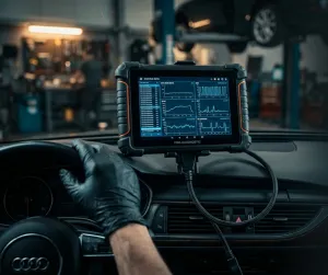
Automotive Diagnostic Scanner Case Study: Designing a Smart OBD-II & CAN Bus Vehicle Analysis Tool
CASE STUDY A technical Automotive Diagnostic Scanner case study from 200,000+ units shipped across multiple ODM lines — covering real architecture decisions, a field failure that rewrote our PCB rules, and the data behind what actually drives returns. 200k+Units Shipped 4.2% → 0.3%Comms Failure Rate 68%RMAs: Missing OEM Data 40–60%Real Enhanced Coverage 1. Project Overview 1.1 Client Background The client was an automotive service equipment brand with an established entry-level OBD tool line — think ELM327-based adapters and basic code readers. They wanted to move up the value chain into professional multi-system scanners. Target market: independent repair shops, fleet maintenance operations, and dealership service bays. Markets in scope from day one were North America and Europe, with Asia as a second-phase target. The gap they were trying to close was real. Entry-level tools read generic powertrain codes. Professional shops need ABS, SRS, transmission, TPMS, bidirectional controls, and live ECU data
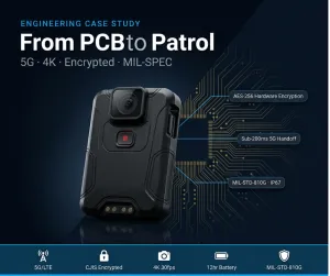
How We Built a 5G Body-Worn Camera From PCB to Patrol: A Real Engineering Case Study
4K recording. Encrypted live streaming. 12-hour battery. Military-grade shell. Here’s what it actually took. The brief landed like most government contracts do: detailed on outcomes, vague on constraints. A public safety equipment supplier needed a next-generation body-worn camera—a 5G body-worn camera, 5G-connected, 4K-capable, encryption-ready, and durable enough to survive whatever law enforcement throws at hardware. Oh, and production-ready. Not a prototype. Not a pilot batch. Volume. This wearable surveillance camera needed to function as a real-time video streaming device. We’d built rugged devices before—body camera OEM projects, industrial wearables, secure IoT hardware, including body camera OEM/ODM programs. But this one had a different pressure to it: chain-of-custody data, CJIS compliance. Officers in the field are depending on footage that might end up in court. Every engineering decision carried legal weight, not just technical weight. This is what the project actually looked like: the tradeoffs, the failures, the decisions that didn’t
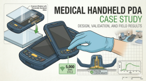
Medical Handheld PDA Case Study: Healthcare-Grade Android Device Development from Concept to Mass Production
The term medical-grade is frequently used as a marketing label to justify high prices for mobile hardware. However, in a hospital ward at 3:00 AM, a device is only as good as its ability to survive “survival use.” This case study explores the development of a medical handheld PDA, moving past brochure specifications to address the chemical, mechanical, and human friction that defines clinical success. Also Read: Rugged Tablet Casestudy 1. Project Overview We partnered with a healthcare integrator to develop a mobile solution for hospital IT system providers. The goal was to replace fragmented, consumer-grade hardware with a single, reliable Android platform designed for the high-intensity hospital workflow. Application Scenarios The device was engineered to serve four critical pillars of hospital operations: Project Objective The client needed a device that could keep working through nonstop hospital use, day and night, for around 5 to 7 years. Because of that,
How We Built a Secure Financial Tablet: An Android OEM Case Study for Banking & Fintech
Executive Summary A regional retail chain needed a PCI-certified, EMVCo-compliant Android tablet for branch-level payment processing. What followed was a $280,000 hardware failure, an 11-week re-spin, and lessons most OEM brochures won’t document. This case study covers the architecture decisions, the failure, the fix, and the security engineering realities that separate a financial tablet from a device that merely passed its certification audit. What Banks Think They’re Buying The truth we tell every client before touching a schematic: PCI PTS, EMVCo L1/L2, Android Enterprise, and MDM compliance are not a security guarantee. They are a liability transfer mechanism. Also read: Rugged Tablet Case Study PTS certification is a snapshot, not a shield. PCI PTS v6 certifies the device at a fixed point in time. Any firmware update — including a security patch — triggers re-certification. Most OEMs lock firmware to avoid re-cert costs. Banking tablets routinely run 18–24 months behind
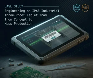
Rugged Tablet Case Study: Engineering an IP68 Industrial Three-Proof Tablet from Concept to Mass Production
Your IP68 rugged tablet passed the lab test. That’s not the same as surviving a logistics warehouse. Between a static IEC 60529 immersion test and a cold-chain distribution center running 24/7, there’s a gap wide enough to kill a program — and most OEM engineers only find it after PVT. Here’s exactly how Wonderful PCB engineered a 10.1-inch 5G three-proof tablet for high-volume warehouse deployment, and what actually went wrong along the way. 1. Project Overview The client operated a Tier-1 logistics network — high-volume distribution centers plus cold-chain facilities handling food and pharmaceutical freight. Their existing consumer-grade rugged tablets were failing within 90 days on the warehouse floor. Screens cracking. Seals leaking after refrigerated truck runs. Wi-Fi dropping near metal racking. The brief was specific: build a 10-inch 5G rugged Android tablet that could handle forklift-mount vibration, concrete drops, daily thermal swings from −25°C freezer bays to 55°C trailer
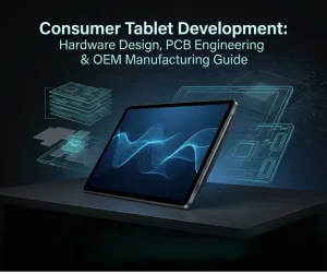
Consumer Tablet Development: Hardware Design, PCB Engineering & OEM Manufacturing Guide
Many brands look at a prototype and think the work is done. This is not true. In tablet manufacturing, the prototype in a factory is often a Golden Sample. First, you need to understand that this sample is made by hand. It uses the best parts. So it works very well. Then start mass production. Same as always, the factory might try to save money by changing parts. This is why you must know the engineering. How do we keep the quality the same for 10,000 units? The Consumer Tablet Market Landscape The market for consumer tablets is growing in many areas. People use them for schools, for smart homes, and for watching movies. You are interested to make own design or use an existing one from a factory. Generally avoid just picking a product from a catalog. In terms of business, it is better to customize. So have a
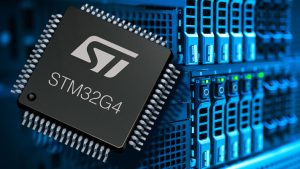
STM32 Microcontroller Firmware Extraction & IC Unlock
Overview of STM32 Microcontrollers STM32 microcontrollers lead industrial, automotive, and consumer electronics devices worldwide. You find these ARM Cortex-M based microcontroller units in motor control systems, building automation, programmable logic controllers (PLCs), medical devices, and countless IoT applications. Their combination of performance, power efficiency, and extensive peripheral choices make them the go-to choice for embedded systems designers. Common applications extend across industries. Industrial automation depends on STM32 for real-time control and communication protocols. Automotive systems utilize them for body control modules, dashboard displays, and sensor interfaces. Consumer products including smart home devices, wearables, and appliances incorporate STM32 microcontrollers for their processing needs. Firmware protection exists for legitimate security reasons. Manufacturers protect their intellectual property from unauthorized copying and competitive analysis. Security-sensitive applications require protection against tampering and malicious code injections. However, legitimate needs for firmware access arise when you maintain legacy equipment, recover lost development files, or perform authorized system
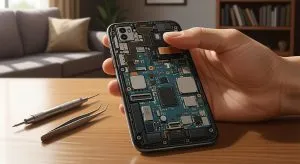
3 simple mobile phone repair tips for motherboard issues
Fix mobile phone motherboard issues with three simple mobile phone repair tips. Save money, avoid common mistakes, and know when to seek expert help.
Why mobile phone motherboards fail and how to prevent it
Mobile phone motherboards fail due to heat, water, and poor charging. Prevent damage with safe habits, quality accessories, and regular maintenance.
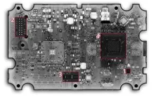
What is a mobile phone motherboard and why is it important?
A mobile phone motherboard connects and controls all key components, ensuring your device runs smoothly and remains reliable over time.

Comparison of mobile phone motherboard suppliers: Alibaba vs. eBay vs. Amazon
Compare mobile phone motherboard suppliers on Alibaba, eBay, and Amazon for certifications, quality, pricing, and buyer protection to choose the best fit.
How to replace a mobile phone motherboard safely at home
Safely replace a mobile phone motherboard at home with step-by-step guidance, essential tools, and tips to protect your device and data during the process.
3D Imaging & PCB X-Ray Tomography for Multi-Layer PCB
You cannot see inside multilayer printed circuit boards with your eyes. X-ray 3D imaging reveals hidden traces and vias that persist invisible to cameras and microscopes. Traditional reverse engineering needs destructive layer separation. You dissolve layers with chemicals, abolishing the original board permanently. Manual de-layering takes more time (weeks) and leaves you with nothing to verify your work against. 3D Imaging X-ray tomography provides non-destructive analysis of all internal Printed Circuit Board structures. The technology advanced from simple 2D X-ray inspection in early 2000s to sophisticated 3D CT scanning systems available in 2026. You preserve the original board completely intact. You see all layers simultaneously with micron-level resolution. Analysis that took weeks now completes in hours with better accuracy. This guide describes how X-ray imaging works for printed circuit board analysis. You will learn the fundamentals of technology, understand the 3D imaging process, know when to use X-ray versus conventional
5G Rugged Smartphone Development
A Technical Case Study from Concept to Mass Production Wonderful PCB | 2026 Edition | Engineering Intelligence Series Most 5G rugged smartphone failures don’t start on a job site. They start in a boardroom when someone says ‘we’ll just add a tough case.’ What follows is a hardware development record from Wonderful PCB — covering real failure data, RF engineering traps, procurement conflicts, and the three parts of a rugged 5G program that consistently go wrong: connectors, antenna detuning, and certification re-spins. Project Background & Client Requirements Why Standard Phones Keep Failing in the Field Construction sites, oil rigs, and mining operations share the same verdict on consumer phones: 3 to 6 months, then dead. The failure modes are consistent: Now layer 5G on top of that. Industrial clients want 5G SA/NSA for low-latency machine communication, IoT, and live video. So the hardware brief becomes: design something that handles all
Flexible PCB & Rigid-Flex PCB Cloning: Complete Reverse Engineering Guide
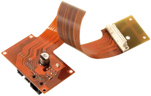
Introduction Flexible printed circuit boards (FPC) and Rigid-Flex printed circuit boards demonstrate advanced circuit board technology that twists, bends and folds to fit unique product designs. You find these bendable circuit boards everywhere in modern electronics, smartphones, wearables, medical devices, and automotive systems. Their ability to adapt to three-dimensional shapes and survive millions of flex cycles makes them irreplaceable in compact, high-reliability applications. Companies need PCB cloning services for several significant reasons. You lost your original design files when a key engineer quit. Your OEM discontinued production, leaving you without replacement boards. Supply chain issues forced you to find alternative manufacturing sources. You need to redesign or upgrade legacy products while maintaining compatibility. These situations demand precise flexible PCB cloning to keep your products in production. Cloning flexible and rigid-flex PCBs needs specialized reverse engineering skills far beyond standard rigid board cloning. The unique materials, complex layer structures, and critical
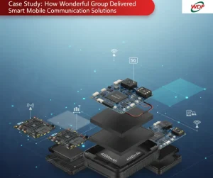
Case Study: How Wonderful Group Delivered Smart Mobile Communication Solutions
A project to build a high-end mobile communication device often feels like a giant puzzle. There are so many tiny pieces that have to fit together. If one part is wrong, the whole thing fails. Wonderful Group took on this challenge and finished a massive project for smart communication equipment. They did not just provide parts. They provided a full path from a simple idea to a finished, working product. This case study looks at how they used their ten years of experience to make this a success. First, you need to see the big picture. Wonderful Group acted as a smart communication equipment solution provider. They did not work alone. They used their status as an official authorized agent for MediaTek to get the best chips. This project focused on using the Dimensity series chips to create a range of powerful devices. Because the project is now complete, we