

Bluetooth Wristbands design and manufacturing
Bluetooth Wristbands design and manufacturing covers features, hardware, software, and quality steps for safe, reliable, and customizable smart wearables.

The design and manufacturing of sports watches
Sports watches combine advanced design, durable materials, and smart features to deliver comfort, accuracy, and style for active lifestyles.
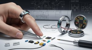
The design and manufacturing of smart rings
Smart Rings combine advanced sensors, durable materials, and compact design to deliver health tracking, payments, and connectivity in a wearable device.

Feature Phones design and manufacturing
Feature Phones offer durable design, affordable pricing, and simple menus. Learn how manufacturing ensures reliability, long battery life, and user-friendly features.

The Essential Process of Designing and Manufacturing Smart Tablets
Smart Tablets are designed and manufactured through R&D, user-centric design, quality assembly, and advanced hardware for reliable performance.

How to Build Smart Devices from Concept to Production
Smart devices go from concept to production with user-focused design, prototyping, and smart manufacturing for quality, efficiency, and innovation.

Battery Management System in electric vehicles
A Battery Management System in electric vehicles ensures safety, extends battery life, and optimizes performance by monitoring and protecting the battery.

Satellite Communication System Design and Manufacturing
Satellite Communication system design and manufacturing ensure reliable, high-performance connectivity through advanced engineering and quality testing.

Onboard Charging Piles design and manufacturing
Onboard Charging Piles design and manufacturing covers safety, efficiency, standards, and installation for reliable electric vehicle charging solutions.

Facial Recognition Door Locks design and manufacturing
Facial Recognition Door Locks offer secure, keyless entry with advanced design, robust manufacturing, and smart home integration for modern security.
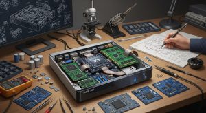
Set-top box design and manufacturing
Set-top box design and manufacturing covers hardware, OS choices, connectivity, PCB layout, and quality control for reliable streaming devices.

4G/5G Wireless Routers Design and Manufacturing
4G/5G Wireless Routers offer robust design, advanced security, and reliable manufacturing for industrial and remote connectivity needs.
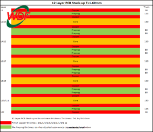
PCB Stack-Up Design for 5G Applications: Layer Configuration and Grounding
1. Introduction 1.1 The 5G Revolution and PCB Challenges The global rollout of 5G wireless technology represents the most significant transformation in telecommunications infrastructure since the advent of 4G LTE. Operating across two distinct frequency bands sub-6 GHz for broad coverage and millimeter wave (mmWave) frequencies ranging from 24 to 77 GHz for ultra-high speed data transmission 5G networks demand unprecedented precision in printed circuit board (PCB) design. Unlike conventional PCB applications, 5G systems must handle signal frequencies where even microscopic design flaws can cause catastrophic performance degradation. According to industry analysis, the global 5G infrastructure market is projected to exceed $47.7 billion by 2027, driving massive demand for high-performance PCB solutions. This growth creates both opportunities and challenges for PCB designers who must master the intricate relationship between material properties, layer configuration, and signal behavior at radio frequencies. The transition from 4G to 5G isn’t merely an incremental upgrade
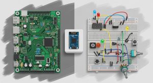
PCB vs breadboard: Which is better for your project?
Choose PCB breadboard for quick prototyping; pick PCB for reliable, lasting circuits. Find the best fit for your project’s needs and goals.

3W rule in PCB design
The 3W rule in PCB design spaces traces at least three times their width to reduce crosstalk and maintain strong signal integrity.

Common PCB design rules
Follow key PCB design rules for reliable, manufacturable boards. Learn spacing, routing, and IPC standards to prevent errors and ensure quality results.

Rules for high speed pcb design
Follow key rules for high speed PCB design to maintain signal integrity, control impedance, reduce noise, and prevent common layout errors.

55 rule in pcb design
The 55 rule in PCB design spaces signal traces five times their width apart, improving signal integrity and reducing EMI and crosstalk.

20H Rule in PCB design for EMI and Signal Integrity
The 20H rule in PCB design reduces EMI and boosts signal integrity by spacing power and ground planes, making your circuits more reliable and compliant.

December Performance Sprint Kickoff — Full Speed Ahead!
As the year draws to a close, our team is fired up and ready to tackle the final stretch with full energy! On [date], we held our December Performance Sprint Kickoff Meeting, marking the official launch of our year-end push to achieve outstanding results. This kickoff was more than just a meeting — it was a moment of inspiration, motivation, and unity. Our leadership team shared clear goals, strategies, and action plans to ensure everyone is aligned and focused on delivering excellence. Why December Matters December is a critical month for our business. It’s the last opportunity to surpass targets, strengthen customer relationships, and set the foundation for an even stronger start to next year. Our team’s dedication and teamwork will be the key to success. Highlights from the Kickoff We captured some of these exciting moments in the video below — watch how our team comes together with passion