You should follow some important PCB design rules. These rules help you make circuit boards that work well. They also make your boards easier to build. If you follow these rules, you can avoid many mistakes. Many designers use IPC standards to help them. Here are some examples:
Standard | Description |
|---|---|
Talks about mechanical and electrical parts for all PCB designs. | |
IPC-6012 | Focuses on how strong and easy to build rigid PCBs are. |
IPC-7351 | Gives tips for land pattern design and where to put parts. |
Use these rules as a checklist. They help you make better PCBs every time.
Key Takeaways
Use IPC standards so your PCB design works well and meets rules. Set up a clear grid and board outline before you put parts down. This makes routing easier and helps you avoid mistakes. Plan your stack-up well to help signals stay strong and control heat. Put important parts down first and keep similar parts together. This lowers noise and makes testing easier. Use good labels and documents to help with assembly and fixing problems faster.
Essential PCB design rules
When you start a new PCB project, you need to follow some basic PCB design rules. These rules help you avoid mistakes and make your board easier to build. Many designers use IPC standards to guide their work. Here is a table that shows some of the most important standards:
IPC Standard | Description |
|---|---|
IPC-2221 | Sets rules for PCB design, including materials, thermal management, and quality. |
IPC-2222 | Gives details for high-voltage boards, like spacing and insulation. |
IPC-6012 | Focuses on rigid PCB reliability and performance. |
IPC-A-600 | Lists what makes a PCB acceptable after fabrication. |
IPC-7351 | Covers land pattern design for surface mount parts. |
IPC-4101 | Explains what materials you can use for PCBs. |
IPC-2615 | Talks about flexible circuit design and manufacturing. |
IPC-6013 | Relates to high-frequency PCB design. |
You should use these standards as a checklist. They help you make sure your board will work well and pass inspection.
Grid setup and board outline
You need to set up your grid before you place any parts. The grid helps you line up components and traces. Most design software lets you pick a grid size. A common choice is 0.1 inch or 2.54 mm. This size matches many standard parts. If you use a good grid, your board will look neat and be easier to route.
Next, you must draw the board outline. The outline shows the shape and size of your PCB. You should make the outline clear and simple. Avoid odd shapes unless you need them for your project. A clear outline helps the manufacturer cut your board correctly. It also helps you fit your board into its case.
Tip: Always check the board outline with your mechanical team or use a 3D viewer in your design software. This step helps you catch mistakes early.
Stack-up and layer planning
You need to plan your stack-up before you start routing. The stack-up is the order of layers in your PCB. Good stack-up planning helps with signal integrity and heat control. Here is a table that shows how stack-up affects your board:
Aspect | Impact on Signal Integrity and Thermal Management |
|---|---|
Layer Structure | Affects signal quality and reduces interference |
Controlled Impedance Paths | Keeps signals clean in high-speed designs |
Heat Management | Helps your board handle heat better |
When you plan your stack-up, follow these steps:
Keep the stack-up balanced. This step avoids stress during manufacturing.
Place ground planes near high-speed signal layers. This setup gives signals a safe path and lowers noise.
Route high-speed signals first. Put them on outer layers or near reference planes.
Use simulation tools to check your design. Test prototypes to find problems like crosstalk early.
Think about manufacturing limits. Material thickness and trace width can change during production.
A good stack-up also helps you avoid common problems. For example, poor layer planning can cause signal loss or heat buildup. You can fix these issues by using solid ground planes and careful layer arrangement.
Many design tools, like Altium Designer and OrCAD, help you follow these PCB design rules. They check your stack-up and flag errors before you send your board to the factory.
Note: If you follow these steps, you set a strong base for your whole design. Good grid setup, board outline, and stack-up planning make every other step easier.
Component placement
Placing must-have components first
Start by putting the most important parts on your PCB. These are connectors, main chips, and power supplies. Put connectors close to the edge so they are easy to reach. Try to place the main chip in the middle of the board. This helps you route signals more easily. Next, add other parts like resistors and capacitors near the main components.
Here is a table that shows what to think about when placing must-have components:
Critical Factor | Description |
|---|---|
Component Grouping | Keep circuits with the same VCC and GND together. |
Function Types | Put analog, digital, and power parts in their own areas. |
Heat Management | Place hot parts next to heat sinks or open spots. |
Voltage & Current | Be careful with high-voltage and high-current parts. |
Placement Order | Start with connectors, then main chips, then other parts. |
Thermal Management | Use thermal vias and let air flow for cooling. |
Grouping and orientation
Group parts by what they do. For example, keep all analog parts together. Keep all digital parts together too. This lowers noise and makes testing easier. Make sure similar parts face the same way. If all resistors point the same direction, you can check them faster when building.
Tip: Grouping and using the same direction for parts helps assembly and testing. Using standard interfaces and strong fasteners also lowers mistakes when building.
Spacing and manufacturability
Follow spacing rules so you do not have problems when making the board. The IPC guidelines say you need space between parts and drill holes. This stops parts from touching and causing shorts. For example, keep at least 16 MIL between holes. If you use less space, you must follow special rules.
Leave enough space between parts for soldering and checking.
Put drill holes away from traces and other parts.
Follow spacing rules for both outside and inside layers.
When you follow these PCB design rules, your board is easier to build and test. Good spacing also helps your board pass quality checks.
Routing rules
Trace width and clearance
You need to choose the right trace width and clearance for your board. Trace width affects how much current a trace can carry. Clearance is the space between traces. Both are important for safety and performance. The minimum clearance depends on voltage, signal speed, and the environment. For example, low voltage circuits need at least 0.1 mm (4 mils) between traces. Power conversion devices need 0.13 mm (5.1 mils). High voltage circuits need at least 1.5 mm (about 60 mils). If you work with high-speed signals, keep the spacing at least three times the trace width. This helps prevent crosstalk and signal problems.
Trace Width (mil) | Recommended Current (A) |
|---|---|
6 | N/A |
10-12 | N/A |
Tip: Always follow IPC 2221 standards for minimum clearance. Adjust your design if you expect high humidity or other tough conditions.
Short, direct routing paths
Keep your traces as short and direct as possible. Short traces help signals travel faster and stay strong. Long traces can act like antennas and cause electromagnetic interference (EMI). EMI can hurt your circuit’s performance. Short, direct paths also lower the risk of signal loss and reflections. This is very important for high-speed designs. You get better results and fewer problems when you keep traces short.
Avoiding crossing nets
Try not to let nets cross each other. Crossing nets can make routing harder and may force you to use more layers or vias. You can avoid this by planning your component placement carefully. Place parts so that related signals do not need to cross. In mixed-signal designs, keep analog and digital traces apart. This helps prevent noise and makes your board easier to route.
Minimize crossing nets during placement.
Use creative part placement to reduce net crossings.
Keep analog and digital areas separate.
Following these PCB design rules will help you make boards that work well and are easy to build.
Power and ground management
Power plane layout
You must plan your power planes well to keep your board working right. Good power plane layout stops voltage drops and noise. There are a few ways to make your design better:
Strategy | Description |
|---|---|
Optimizing Trace Width and Copper Thickness | Pick wide traces and thick copper. This lowers resistance and keeps voltage steady. |
Adjacency Principle | Put power and ground planes next to each other. This helps lower noise and controls EMI. |
Include Bulk Capacitors | Add bulk capacitors to keep voltage steady and cut down power noise. |
Tip: Use a thin layer between power and ground planes. This makes more plane capacitance and helps with decoupling.
Ground plane practices
A solid ground plane is very important for a strong PCB. It gives return currents a path with low resistance. This lowers noise and keeps signals clean.
Make your ground plane one piece. Do not break it up.
Use stitching vias to join ground planes when signals move between layers.
Keep loop areas small to lower EMI and block outside noise.
Think about every signal and its return path as a closed loop.
A good ground plane helps your board pass EMI tests and keeps signals strong.
Decoupling capacitors
Decoupling capacitors help protect your circuit from voltage spikes and noise. You should do these things to place them well:
Give each power rail its own decoupling capacitors.
Use more than one via to connect capacitors to power and ground planes.
Put capacitors close to the power plane with short vias.
Connect the component pin to the capacitor first, then to the via.
Use parallel resistors with capacitors to filter out high-frequency noise.
Sometimes, put capacitors in series with I/O traces to block DC.
When digital chips switch, they need quick bursts of current. Short rise times mean higher current. You must keep impedance low so your board can give this current fast. This is one of the most important PCB design rules for stable circuits.
Signal integrity
High-speed design guidelines
You need to keep signals safe in high-speed circuits. Good signal integrity helps your board work well. Here are some steps you should follow:
Match trace impedance to the source and load. This lowers signal reflections.
Use controlled impedance for high-speed traces. This keeps signals steady.
Make traces short to cut down delay and noise.
Do not use sharp corners. Use smooth bends in trace paths.
Keep trace widths the same. This helps keep impedance steady.
Space traces apart to stop cross-talk.
Use differential pair routing for signals that need it.
Put ground and power planes under high-speed traces.
Keep the return path short and direct for signals.
Tip: Put decoupling capacitors close to power pins. Use different values to block many types of noise.
Controlled impedance
You get controlled impedance by matching board material with trace size and location. This keeps signal impedance in a safe range. Most PCB traces need impedance between 25 and 125 ohms. Try to keep tolerance within plus or minus 10%. Steady impedance stops reflections and keeps signals clean. Always check your design with your manufacturer to meet these values.
Reducing EMI and crosstalk
Electromagnetic interference (EMI) and crosstalk can cause problems in your circuit. You can lower EMI by making loop areas small. Route high-speed traces close to their return paths. Do not split ground planes. Use vias carefully to keep inductance low.
You can also:
Use ground planes to give current a safe path and make loop area smaller.
Space signal traces apart to lower crosstalk.
Use differential pairs for high-speed signals to cancel noise.
Put decoupling capacitors near IC power pins.
Add shielding, like metal covers, to block EMI.
If you follow these PCB design rules, your signals will stay strong and your board will be reliable.
Labeling and documentation
Font size for readability
You need to make sure that everyone can read the text on your PCB. Good labeling helps you and others find parts quickly. If you use the right font size, you avoid mistakes during assembly and repair. The IPC standards give clear rules for silkscreen text. You should follow these measurements:
Font Size Type | Measurement |
|---|---|
Minimum Font Height | 0.040 inches (40 mils) |
Minimum Stroke Width | 0.006 inches (6 mils) |
Ideal Font Height for High Visibility | 0.050 to 0.060 inches (1.27 to 1.524 mm) |
Maximum Font Height | Avoid exceeding 0.080 inches (2.032 mm) unless space permits |
If you use a font height between 0.050 and 0.060 inches, you make your labels easy to see. Try not to use fonts smaller than 0.040 inches. Small text can fade or blur during manufacturing. Large text can take up too much space and cover important pads. You should also keep the stroke width at least 0.006 inches. This keeps the letters clear and sharp.
Tip: Always check your silkscreen in the design software’s preview. This helps you spot text that is too small or too close to other features.
Clear component labels
Clear labels help you build and fix your board faster. When you use good silkscreen markings, you can find parts quickly during testing. You also lower the chance of mistakes when you put the board together. Here is how clear labels improve your work:
Evidence Description | Impact on Efficiency |
|---|---|
Clear silkscreen markings allow quick location of components during debugging. | Saves hours during fault diagnosis. |
Thoughtful silkscreen design reduces misinterpretation of assembly instructions. | Ensures accurate translation of design. |
Following guidelines can reduce assembly errors by up to 30%. | Particularly in manual assembly. |
Strategic placement of labels aids in quick identification on high-density boards. | Enhances ease of use at a glance. |
Simple additions can lower manual assembly time by 15-20%. | Reduces likelihood of errors requiring rework. |
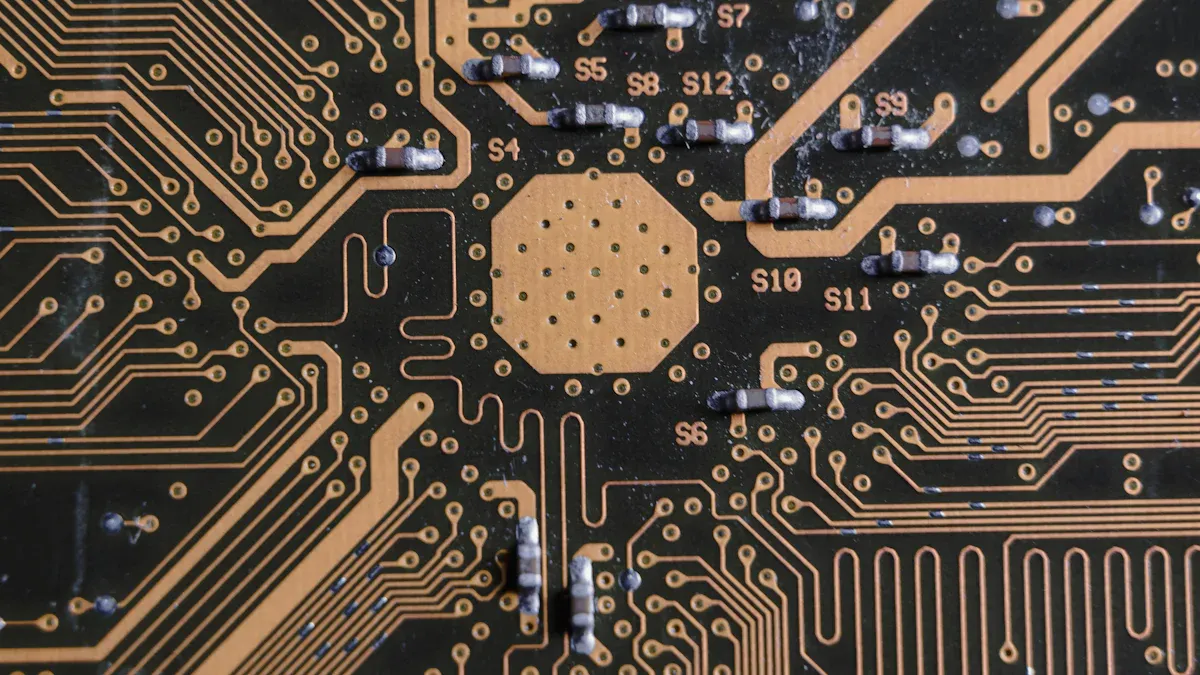
You should place labels next to their parts, not under them. This makes them easy to see after assembly. Use short, clear names like R1, C2, or U3. If you follow these PCB design rules, you make your board easier to use and repair. Good documentation also helps others understand your design.
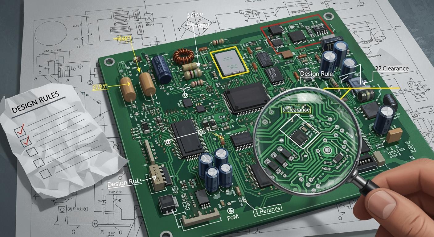
Design rule checks and manufacturing prep
Setting DRC parameters
You must set up your Design Rule Check (DRC) parameters before making your board. DRC parameters help you find mistakes early. They make sure your design follows rules and your manufacturer’s needs. Here is a table that shows the most important DRC parameters and why they matter:
DRC Parameter | Definition | Importance | Guideline |
|---|---|---|---|
Clearance Rules | Minimum space between traces, pads, and copper pours. | Stops shorts and signal problems. | Use IPC-2221 or manufacturer’s minimums (like 4 mil for standard PCBs). |
Trace Width Rules | Smallest allowed width for traces. | Prevents overheating and keeps signals strong. | Use IPC-2152 charts to pick the right width for your current. |
Via and Drill Rules | Smallest drill size and space between vias. | Keeps connections strong and easy to make. | Standard via drills are at least 0.3 mm. |
Pad Size and Annular Ring | Copper ring around a drilled hole. | Makes component leads stronger. | Keep at least 4–5 mil annular ring. |
Solder Mask Rules | Space around pads and traces in the solder mask. | Stops solder bridges and shorts. | Minimum mask slivers should be 4 mil or more. |
Component Placement Rules | Space between parts and from board edges. | Avoids mechanical problems and helps soldering. | Keep tall parts away from connectors; use at least 40 mil edge clearance. |
High-Voltage Clearance and Creepage | Space for high-voltage designs. | Stops arcing and meets safety rules. | Follow IEC 60950-1 for creepage distances. |
Differential Pair Rules | Matched routing for pairs like USB or HDMI. | Keeps signals clean and lowers noise. | Match lengths within 5–10 mil and control impedance. |
Length Matching and Timing Rules | Makes sure signals arrive together. | Stops timing errors. | Use serpentine routing to match trace lengths. |
Thermal Relief and Copper Balance | Helps heat move away and keeps copper even. | Stops warping and helps soldering. | Use thermal relief pads and balance copper pours. |
Setting these parameters helps you avoid expensive mistakes. It also makes your board easier to build.
Common DRC violations
You might see some common DRC violations when you check your design. These problems can make your board fail or hard to build. Here is a table that shows the most frequent violations and how to fix them:
Common Violation | Description | DRC Solution |
|---|---|---|
Insufficient Trace Clearance | Traces are too close and may short out. | Set proper clearance rules based on voltage. |
Incorrect Trace Widths | Traces are too thin or too thick. | Define trace width rules for the right current. |
Misaligned or Improperly Sized Vias | Vias are too small or not lined up. | Set rules for via size and spacing. |
Inadequate Solder Mask Clearance | Not enough space in the solder mask. | Define solder mask clearance to stop solder bridges. |
Board Edge Proximity Issues | Copper is too close to the edge. | Enforce edge clearance rules. |
Signal Integrity Violations | High-speed signals are not routed well. | Use rules for differential pairs and impedance control. |
Automated DRC tools help you find these errors quickly. Fixing them early makes building easier and lowers the chance of delays.
Generating manufacturing files
After you pass all DRC checks, you need to get files ready for manufacturing. Most PCB makers want these file types:
Gerber Files: Show each layer of your PCB.
ODB++: Combines all data for making your board.
Bill of Materials (BOM): Lists every part on your board.
Centroid (Pick-and-Place) File: Shows where each part goes and its rotation.
IPC-2581: Packs all fabrication and assembly data into one file.
Always check your files before sending them. Use design validation tools and advanced inspection methods like AOI or X-ray testing to catch any last mistakes.
You should follow these steps to get your board ready for production:
Export your PCB layout using your manufacturer’s rules.
Run automated DRCs to check for mistakes.
Do electrical rule checks (ERCs) to make sure all connections work.
Make sure your design meets industry standards and project needs.
Quality control is very important in PCB fabrication. Careful checking and good files help you make boards that work well and pass all tests. Following PCB design rules at every step makes building and using your board easier.
When you use PCB design rules, your boards are safer. They are also easier to build. You make fewer mistakes and save money. Automation tools help you find problems early. Good planning means you do not waste money fixing errors.
Aspect | Description |
|---|---|
Automation | Software checks if your design follows the rules. |
Early Checks | You spot problems before making the board. |
Cost Savings | You do not spend extra money fixing mistakes. |
Picking good materials helps your boards last longer. Planning for heat and stress makes them stronger. Your boards work better and break less often. Keep learning new ways to design. This helps you make even better boards.
FAQ
What is the most important PCB design rule?
You should always keep enough space between traces and pads. This rule helps you avoid short circuits and makes your board safer. Good spacing also helps your board pass inspection.
How do you choose the right trace width?
You need to check how much current your trace will carry. Use IPC-2152 charts or online calculators. Wider traces carry more current and stay cooler.
Why do you need a ground plane?
A ground plane gives signals a safe path. It lowers noise and keeps your board stable. You also make your board pass EMI tests more easily.
What files do you send to a PCB manufacturer?
You send these files:
Bill of Materials (BOM)
Pick-and-place file
Always check with your manufacturer for their file requirements.