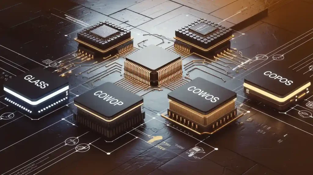
You use rf pcb when you need to work with fast signals. Fast pcb circuits need extra care to keep signals strong. In rf pcb design, you face problems like signal strength, impedance, and noise. You must pay close attention to pcb layout and materials for fast signals. Microwave pcb and rf circuits both need special design steps. You must plan each pcb layer, trace, and ground for good results. Many rf and microwave pcb projects do not work without the right design steps.
Key Takeaways
Make your RF signals strong by using short and wide traces. Keep the traces direct and use smooth bends. This helps stop signal loss and noise.
Match impedance by planning trace width and spacing. Also, plan the layer stack-up. This stops signal reflections and errors.
Use a solid ground plane under RF traces. Do not break the ground plane. This gives a clear return path. It also lowers noise and controls impedance.
Put RF components close to each other. Keep them away from digital parts. This lowers interference and keeps signals clean.
Test your RF PCB well with the right tools. Simulate your design early. This helps you find problems before you make the board.
High-Frequency PCB Principles

Signal Integrity
You need to protect your signals when you work with high-frequency pcb circuits. Signal integrity means your signals stay strong and clear as they travel across the pcb. If you do not plan your rf pcb layout well, signals can lose strength or pick up noise. This can cause your rf circuit to fail.
High-frequency signals move fast. They can reflect, bend, or even leak into other parts of your pcb. You must keep traces short and direct. You should avoid sharp corners. Wide traces help lower resistance and keep your signals clean.
Tip: Use the right materials for your microwave pcb. Materials with low loss and stable properties help keep your signals strong.
You should also keep your rf and digital sections apart. This helps stop noise from digital parts from hurting your rf signals. Good signal integrity makes your rf pcb work better and last longer.
Impedance Matching
Impedance matching is key in high-frequency pcb design. Impedance is like the resistance your signal faces as it moves. If the impedance does not match between your source, trace, and load, your signal can bounce back. This is called reflection. Reflections can weaken your signal and cause errors.
You must plan your trace width and spacing to match the needed impedance. Many rf pcb designs use a 50-ohm trace. You can use calculators or simulation tools to set the right values. The stack-up of your pcb layers also affects impedance. The distance between the trace and the ground plane changes the impedance.
Note: Always check your impedance after you finish your layout. Small changes in your microwave pcb can change the impedance.
Impedance matching helps your rf signals move smoothly. It keeps your high-frequency circuits working as they should.
Ground Planes
The ground plane is one of the most important parts of any high-frequency pcb. You need a solid ground plane under your rf traces. This gives your signals a clear signal return path. It also blocks noise and stops signals from leaking into other parts of your pcb.
You should use a full ground plane layer in your rf pcb. Do not break up the ground plane with too many traces or vias. Gaps in the ground plane can cause noise and signal loss. In microwave pcb design, a strong ground plane helps control impedance and keeps your signals safe.
Here are some tips for using ground planes in high-frequency pcb design:
Place the ground plane right under your rf traces.
Connect all ground points to the main ground plane.
Avoid splitting the ground plane into small islands.
Use many vias to connect the top and bottom ground planes.
Good Practice | Why It Matters |
|---|---|
Solid ground plane | Stops noise and keeps signals strong |
Short traces | Reduces signal loss |
Wide traces | Lowers resistance |
Careful stack-up | Controls impedance and performance |
Remember: The ground plane is not just a place for ground pins. It is a shield and a guide for your high-frequency signals.
Material choice and stack-up also play a big role in high-frequency pcb performance. Choose materials with low loss for your microwave pcb. Plan your layer stack-up so that each rf trace has a ground plane close by. This keeps your impedance steady and your signals clean.
RF PCB Design Process
Designing a high-frequency PCB takes careful planning. You need to follow a clear process to get the best results. Each step helps you avoid problems and build a strong RF circuit.
Schematic Planning
Start your RF PCB design with a good schematic. You need to show every part and connection in your circuit. Place your RF blocks and digital blocks in separate areas. This keeps noise from digital parts away from your high-frequency signals.
You should use clear labels for all signals and power lines. Mark the RF paths so you can spot them easily later. Good schematic planning helps you see where you need special care for RF signals.
Tip: Use simulation tools at this stage. You can check your circuit for signal loss or interference before you start the layout.
Component Placement
Place your components with care. Keep all high-frequency parts close together. This reduces the length of your RF traces. Short traces help keep your signals strong.
Put sensitive RF components away from noisy digital chips. Group similar parts together. For example, keep all filters in one area and all amplifiers in another. Place connectors and antennas at the edge of the PCB for easy access.
You can use the following checklist for component placement:
Keep RF and digital sections apart
Place high-frequency parts close to each other
Avoid placing components over split ground planes
Leave space for tuning or testing points
Trace Routing
Trace routing shapes how your signals move across the PCB. Use straight, short traces for all high-frequency signals. Avoid sharp corners. Use gentle bends or 45-degree angles instead.
Keep your RF traces away from digital traces. This stops noise from leaking into your RF paths. Use wide traces for high-frequency signals. Wide traces lower resistance and help keep your signals clean.
You can use microstrip or stripline routing for controlled impedance. These methods help you match the impedance of your traces to your circuit needs.
Note: Always check your trace width and spacing. Use a calculator or simulation tool to make sure you meet your design goals.
Layer Stack-Up
The layer stack-up is the order of layers in your PCB. A good stack-up helps control impedance and reduce noise. Place a solid ground plane right under your RF traces. This gives your signals a clear return path.
You can use a four-layer PCB for many high-frequency designs. For example:
Layer | Purpose |
|---|---|
1 | RF signals |
2 | Ground plane |
3 | Power plane |
4 | Digital signals |
Keep your RF traces close to the ground plane. This helps you control impedance and protect your signals. Choose materials with low loss for your stack-up. Good materials keep your high-frequency signals strong.
Via Management
Vias connect different layers in your PCB. You need to use them with care in high-frequency designs. Each via adds a small amount of resistance and inductance. Too many vias can weaken your RF signals.
Use as few vias as possible on your RF traces. When you need to cross layers, keep the via path short. Place ground vias near your RF traces to give signals a fast return path.
Alert: Avoid placing vias in the middle of high-frequency traces. This can cause signal loss or reflections.
You can use simulation tools to check how vias affect your signals. Good via management helps you keep your RF PCB working at top performance.
RF PCB Pitfalls
Layout Errors
You can face many problems if you do not plan your high-frequency layout well. One common mistake is breaking up the ground plane. This can cause noise and signal loss. You should keep the ground plane solid under your high-frequency traces. Long or winding traces also hurt your signals. Short, straight traces work best for high-frequency signals. Placing digital and rf parts too close together can cause interference. You need to keep these sections apart on your pcb.
Tip: Always double-check your layout for unwanted trace crossings or sharp corners. These can cause signal reflections in high-frequency circuits.
Material Issues
Choosing the wrong materials can ruin your high-frequency pcb. Some materials absorb signals or change their properties at high frequencies. You should pick materials with low loss and stable performance. If you use cheap or unknown materials, your rf pcb may not work as planned. The thickness of the board and the type of dielectric also affect your signals.
Here is a quick table to help you remember what to check:
Material Factor | Why It Matters for High-Frequency |
|---|---|
Dielectric constant | Controls impedance |
Loss tangent | Affects signal strength |
Board thickness | Changes trace impedance |
Testing Challenges
Testing high-frequency circuits is not easy. Regular test tools may not show all problems in your rf pcb. You need special equipment to measure high-frequency signals. If you skip proper testing, you might miss hidden issues like signal loss or interference. You should test your pcb at the same frequencies it will use in real life. Always check for signal reflections and noise.
Alert: Never skip the testing step. Careful testing helps you catch problems before your rf pcb goes into use.
RF PCB Best Practices
Manufacturability
You should think about manufacturability at the start. Planning for easy rf pcb manufacturing saves time and money. Pick board sizes and shapes that are common. Use parts that are simple to buy. Do not use tiny gaps or very thin traces. These can make problems during making. Talk to your manufacturer to check if your pcb fits their rules. Ask them for their design tips. This helps you avoid waiting for fixes.
Tip: Always check your design for space between parts. This step helps you find mistakes before sending files to the factory.
Simulation Tools
Simulation tools let you see how rf signals will act before building. You can use these tools to test trace width, impedance, and signal paths. Try to run simulations after you finish your schematic and layout. This step helps you find problems early. You can fix signal loss or reflections before making your pcb. Many tools let you model your stack-up and materials. This gives you a better idea of how your board will work.
Use simulation to check:
Impedance matching
Crosstalk between traces
Documentation
Good documentation makes your rf pcb project easier to build and test. You should make clear drawings and notes for every part. Label all rf paths and test points. Add a bill of materials with part numbers. Write assembly notes for special parts. Good documentation helps your manufacturer and test team understand your design. This step lowers mistakes and speeds up making your board.
Document Type | Why It Matters |
|---|---|
Schematic | Shows all connections |
Layout drawing | Guides assembly |
Bill of materials | Lists all parts |
Remember: Clear documentation is just as important as good design. It helps everyone work together.
You have learned the key steps for strong RF PCB layout. Start with careful planning and keep your signals clean. Use solid ground planes and match impedance for better performance. Always check your work and test your board. Pay close attention to every detail. When you follow best practices, you build better RF circuits. Keep learning about RF and PCB design to improve your skills.
Remember: Careful design and testing help you avoid costly mistakes in your next RF project.
FAQ
What is the main difference between RF PCB and regular PCB?
RF PCB is used for high-frequency signals. Regular PCB does not need to worry much about signal loss. RF PCB needs special materials and careful trace planning.
Why do you need impedance matching in RF circuits?
Impedance matching lets RF signals move without bouncing back. If you do not match impedance, signals can bounce and cause problems. Matching impedance keeps your circuit working well.
How do you reduce noise in RF PCB design?
You can lower noise by using a solid ground plane. Keep RF traces short. Put digital and RF parts in different places. Use shielding if you need it. Good layout choices help keep signals clean.
What materials work best for RF PCB projects?
Pick materials with low loss tangent and steady dielectric constant. FR-4 is okay for some low-frequency RF circuits. For higher frequencies, Rogers or Teflon work better.