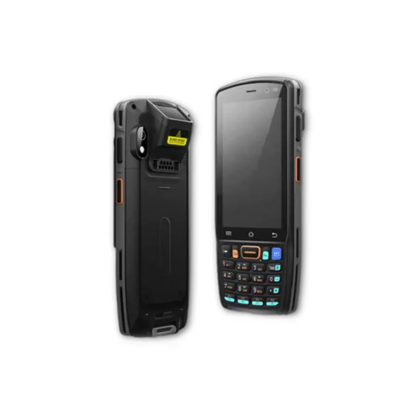
A Technical Case Study from Concept to Mass Production
Wonderful PCB | 2026 Edition | Engineering Intelligence Series
Most 5G rugged smartphone failures don’t start on a job site. They start in a boardroom when someone says ‘we’ll just add a tough case.’ What follows is a hardware development record from Wonderful PCB — covering real failure data, RF engineering traps, procurement conflicts, and the three parts of a rugged 5G program that consistently go wrong: connectors, antenna detuning, and certification re-spins.
Project Background & Client Requirements
Why Standard Phones Keep Failing in the Field
Construction sites, oil rigs, and mining operations share the same verdict on consumer phones: 3 to 6 months, then dead. The failure modes are consistent:
- Charging ports corrode from metallic dust and constant moisture exposure
- Screens crack — not from one big drop, but from 30 small ones over rough terrain
- Batteries lose 30–40% capacity in sub-zero conditions because lithium-polymer cells aren’t rated for it
- Touchscreens stop responding to wet hands or gloves, creating safety hazards
- GPS signal weakens under steel canopies and equipment blockage
- Consumer IP ratings — even genuine ones — degrade within 6 to 12 months of actual field use
Now layer 5G on top of that. Industrial clients want 5G SA/NSA for low-latency machine communication, IoT, and live video. So the hardware brief becomes: design something that handles all of the above while staying waterproof, shockproof, and carrier-certified. That’s a very different engineering problem than making a slim consumer flagship.
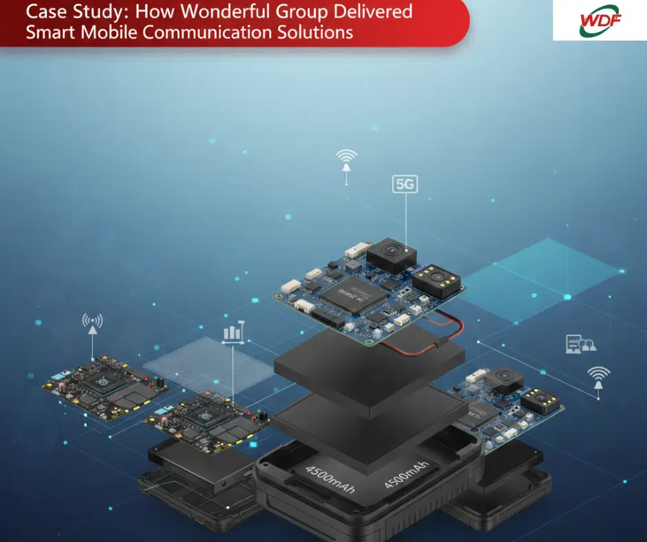
→ Related: Case Study: How Wonderful Group Delivered Smart Mobile Communication Solutions
Core Technical Requirements
A typical client brief for a custom 5G industrial rugged phone includes:
• 5G Sub-6 GHz (SA/NSA) with carrier aggregation
• IP68 and IP69K dual waterproof certification
• MIL-STD-810H compliance — with test report, not just a sticker
• 1.5 to 2.0 m drop resistance onto concrete
• 6,000 to 8,000 mAh battery with fast charging
• Glove-touch and wet-hand display operation
• 1,000+ nit outdoor display
• Optional: NFC, precision GPS, integrated barcode scanner, thermal imaging port
• Android 13 or 14 with MDM compatibility
→ Related: PCBA Design Services — Wonderful PCB
Hardware Architecture Design
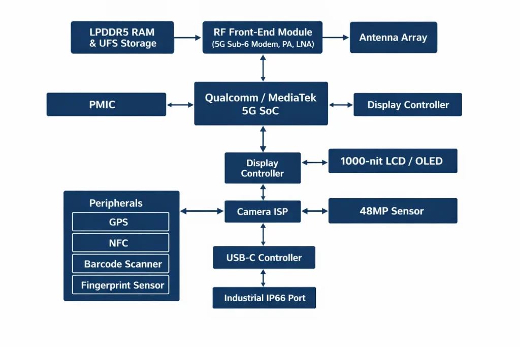
Figure 1: System architecture block diagram of a 5G rugged industrial smartphone — SoC, RF front-end, power management, sensor cluster, and connectivity stack.
Choosing the Right 5G Platform
Qualcomm vs. MediaTek is not a question of which is better. It’s a question of what the program actually needs.
| Criterion | Qualcomm Snapdragon (X-series modem) | MediaTek Dimensity (5G) |
| 5G Band Coverage | Wider global band support; stronger mmWave ecosystem | Strong sub-6 GHz; limited mmWave |
| Thermal Output | Higher peak TDP — needs active thermal management inside sealed enclosures | Lower average TDP; more manageable in thick housings |
| BOM Cost | 15–25% more expensive at volume | More competitive for mid-range programs |
| Software & Drivers | Mature enterprise support; Qualcomm AI Engine | Improving; strong for APAC carrier certifications |
| Best Fit | High-performance industrial, defense-adjacent, global export | Logistics, retail, APAC-focused deployment |
For programs shipping to Europe or the Middle East, Qualcomm’s carrier certification breadth is a real advantage. For APAC logistics at high volume, MediaTek’s cost profile wins.
RF and Antenna Design Inside a Rugged Housing
This is where programs quietly die before anyone notices.
Junior RF engineers — and some rushed ODM teams — treat the thick rugged housing like a thin consumer back cover. Big mistake. At 0.6 to 0.8 mm, polycarbonate is essentially transparent to RF. At 2 to 4 mm, with internal ribs and sealing membranes, it is not.
The housing’s dielectric constant pulls the antenna’s resonant frequency downward by 150 to 400 MHz and adds 2 to 6 dB of insertion loss across mid-band 5G (n77/n78, around 3.5 GHz). Engineers who catch this late try to fix it at the matching network. It doesn’t work. You can correct the frequency shift. You cannot recover the insertion loss that way.
Field Result: Prototypes where housing effects weren’t modeled in HFSS or CST showed 8 to 12 dB worse Total Radiated Power (TRP) and Total Isotropic Sensitivity (TIS) in chamber testing versus bare-board measurements. That’s a failed OTA test — every time.
The fix has to happen before tooling opens. Antenna placement, housing geometry, and material choices all need to be locked at the Industrial Design (ID) stage. Options include placing antennas near enclosure edges with air gaps, using dielectric-compensated designs, or cutting slots in the housing (which then creates a sealing problem). None of these can be retrofitted cheaply after the mold is cut.
PCB and PCBA Design Challenges
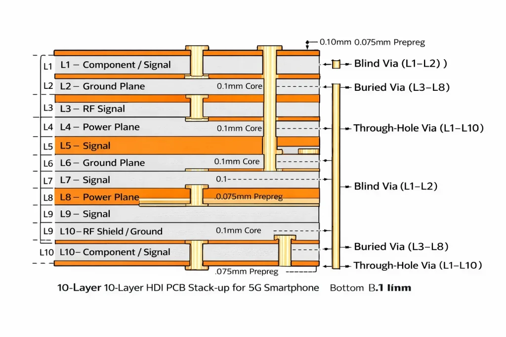
Figure 2: Representative 10-layer HDI PCB stack-up for a 5G rugged smartphone — signal layers, ground planes, RF shielding zones, and via structure.
A 5G rugged smartphone PCBA is not a scaled-up consumer board. The constraints are different:
• 8 to 12 layer HDI stack — needed to route the 5G modem, RF front-end, and power management ICs in a compact footprint
• Heat has nowhere to go in a sealed housing. Copper heat spreaders and graphite sheets are standard. High-performance programs sometimes require vapor chambers for sustained 5G throughput
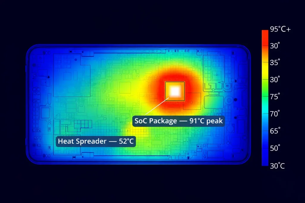
Figure 3: Thermal simulation (FEA) of a 5G rugged smartphone under sustained 5G load at +45°C ambient — hotspot at SoC package, heat spreader distribution path visible.
• 6,000 to 8,000 mAh batteries with 30 to 65W fast charging need dedicated thermal and EMI planning — not an afterthought
• Connectors need IP-rated sealing interfaces at the board level, not just at the housing
• Defense-adjacent applications add MIL-STD-461 EMC requirements that directly compete with 5G antenna placement
Mechanical and Structural Engineering
Waterproof, Dustproof, Shockproof — The Three-Proof Design
Getting IP68/IP69K and MIL-STD-810H all on the same device requires structural decisions that affect cost, schedule, and failure rates downstream.
• Sealing: Dual-layer silicone gaskets at all enclosure joints; acoustic mesh membranes for speaker and mic ports; UV-cured adhesive around the display perimeter
• Frame: Internal magnesium-alloy or aluminum sub-frames add rigidity without excessive weight. How the sub-frame distributes impact energy across the enclosure directly shapes drop survival rates
• Drop simulation: FEA in ANSYS or similar tools should run before any physical prototype. Models need to include angled drops and temperature-affected material properties — not just flat face-down impacts
Wonderful PCB Field Data: One program paired Gorilla Glass Victus with a polycarbonate outer bezel. Lab drops (1.5 m onto steel per MIL-STD-810H Method 516.8) passed cleanly. On construction sites — concrete and gravel — the polycarbonate bezel flexed just enough to transfer shear force to the glass edges. Micro-cracks formed. After 20 to 50 cumulative drops, screens failed. Lab failure rate: below 5%. Simulated field abuse failure rate: 35%.
The fix: swap to a magnesium-alloy sub-frame with controlled flex gaps. That required re-opening molds, re-running EMC and RF qualification, and cost 8 to 10 weeks and roughly 12 to 18% more per-unit BOM. Caught at pilot production — not EVT. That timing is what made it expensive.
Certification Standards: What They Actually Test
IP68 vs. IP69K
• IP68: Continuous immersion beyond 1 metre. Specific depth and duration are manufacturer-defined — for industrial devices, usually 1.5 m for 30 minutes, per IEC 60529
• IP69K: High-pressure, high-temperature water jets — 80 bar, 80°C, 14 to 16 L/min, at 0.1 to 0.15 m distance. Needed for food processing, agriculture, and heavy industrial washdown
• Both ratings are tested on new, undamaged devices in a lab. Real-world IP performance at 12 to 18 months — after gasket wear, adhesive fatigue, and repeated dirty-environment plugging — is substantially lower
MIL-STD-810H: What It Actually Certifies
The hard truth: MIL-STD-810H is not a pass/fail standard with fixed requirements. It is a menu of roughly 30 test methods. Manufacturers choose which ones to run, how many cycles, and at what severity levels. There is no minimum. A phone can claim MIL-STD-810H compliance after running three methods at low severity on a three-unit sample. That is technically accurate. It is also almost meaningless.
When evaluating compliance claims, buyers should ask for the full test report and look for:
• Which exact method numbers and procedure variants were used
• Tailoring parameters — drop height, surface material, number of drops, orientation sequence
• Sample size per test (three units is not statistically meaningful)
• Post-test functional failure rate across the full sample
• Whether combined stressor testing ran — for example, drops at -20°C after a thermal soak
Thermal and Environmental Testing
• Operational temperature range: -20°C to +60°C; storage from -40°C to +70°C
• Thermal cycling under load: 5G modem stays active throughout the temperature cycle — this is how you find real thermal failures, not passive cycling
• Humidity: 95% RH at 40°C for extended exposure periods
• Salt spray: 5% NaCl solution per IEC 60068-2-11 — essential for marine and coastal industrial deployments
Firmware and Software Optimization
Android Customization for Industrial Use
• Custom launcher with larger touch targets and high-contrast modes for glove operation
• Aggressive background management, GPS duty cycling, and 5G/LTE fallback logic to extend field battery life
• Staged OTA update system with rollback support — needed when 50,000 devices in the field can’t be manually updated
• Custom thermal profiles to hold 5G throughput in high-ambient-temperature environments
Security and Enterprise Features
• Hardware-backed encryption via Android Keystore and Trusted Execution Environment (TEE)
• MDM compatibility: Microsoft Intune, VMware Workspace ONE, SOTI MobiControl
• Secure boot chain from bootloader through OS
• Remote wipe and device lock for field security
Prototyping and Testing Phase
EVT, DVT, PVT — What Each Stage Actually Tests
• EVT (Engineering Validation Test): Bring up the SoC. Measure RF on bare board. Validate the power subsystem. Check thermals. Goal: find design errors before spending on tooling
• DVT (Design Validation Test): Full device in final or near-final housing. This is where drop, IP immersion, RF OTA in anechoic chamber, display optical measurement, and battery cycle testing happen. Goal: confirm the design hits every spec
• PVT (Production Validation Test): Pilot production run. Checks process capability, yield, and functional test line performance. Goal: confirm the factory can build it consistently
Reliability Testing Protocol
• Drop test: Minimum 26 drops per unit per MIL-STD-810H Method 516.8, plus 500+ cumulative impact tumble testing on a 50-unit cohort
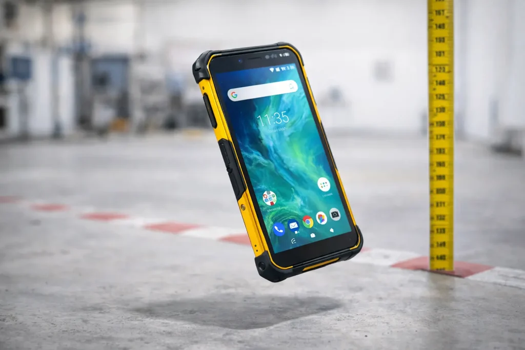
Figure 4: 2.0 m concrete drop test during DVT phase — device orientation per MIL-STD-810H Method 516.8.
• Waterproof: IP68 and IP69K per IEC 60529, re-tested after 500 drops to check seal integrity under abuse conditions
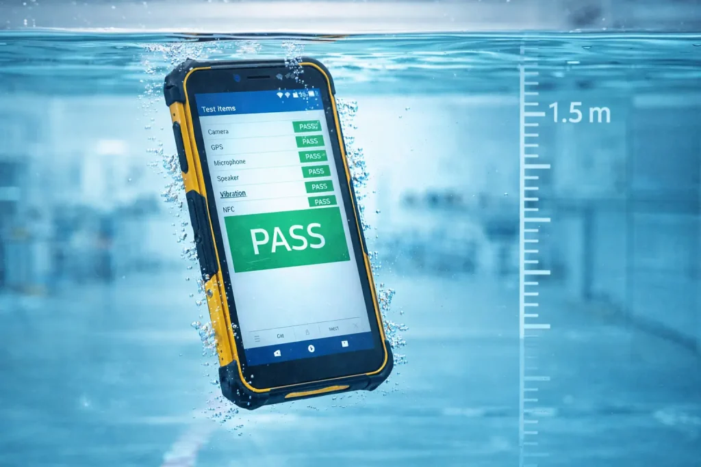
Figure 5: IP68 immersion test — device submerged at 1.5 m depth, 30-minute soak, functional operation confirmed post-test.
• Button durability: 300,000+ actuations on all mechanical buttons
• USB-C port: 10,000+ insertion/withdrawal cycles, then salt-fog exposure, then re-test for waterproofing
• Thermal cycling under load: 100+ cycles across the full operational temperature range with the 5G modem active
Mass Production and Supply Chain Management
Component Procurement
Here’s where the differences actually count:
• 5G modules: Long-lead items requiring early procurement and second-source qualification. Post-2020 geopolitical supply disruptions hit 5G modem lead times harder than almost any other component category
• USB-C connectors: Industrial IP-rated USB-C connectors cost 2 to 4x more than consumer equivalents. Programs that swap in cheaper connectors to cut BOM cost see field failure rates of 18 to 28% at 12 to 18 months (Wonderful PCB field data). Industrial connectors bring that below 6%.
• Battery cells: 6,000 to 8,000 mAh cells for -20°C operation need industrial or automotive-grade cell chemistry. Consumer lithium-polymer loses 30 to 40% capacity at -10°C
• Display assemblies: 1,000+ nit panels with glove-touch and wet-hand controllers have longer lead times than standard panels — source them early
SMT and Assembly
• Fine-pitch BGA placement for 5G SoC packages; AOI after each paste and reflow stage
• Selective conformal coating (acrylic or silicone) on the PCBA for moisture and corrosion protection beyond the housing seal
• Clean bench assembly for camera module and display integration to stop particulate contamination
• Production line includes RF OTA spot-checks, charging circuit tests, display uniformity, button function, and IP immersion sampling
Quality Control System
• AOI: Post-paste and post-reflow inspection for solder defects
• X-ray: BGA solder joint verification on every 5G SoC package
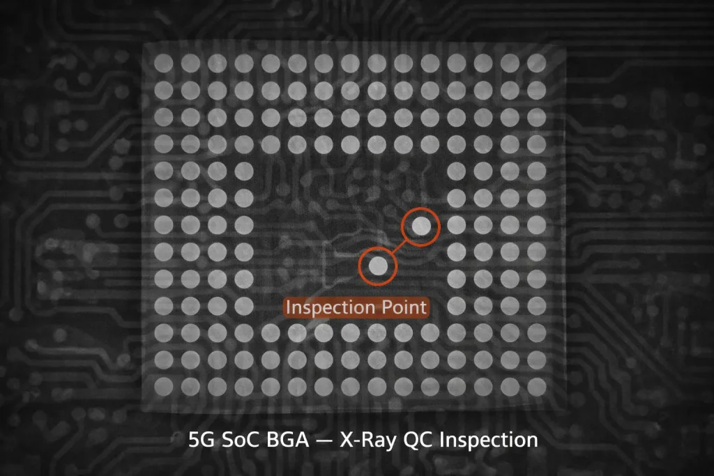
Figure 6: X-ray inspection of BGA solder joints on 5G SoC package — voiding and bridging detection on production PCBA.
• Burn-in: 24 to 48 hours powered operation at elevated temperature to screen early-life failures

Figure 7: Production burn-in aging test — devices powered at elevated temperature for 48 hours to screen early-life failures before shipment.
• Final audit: AQL sampling per IEC 60068; IP immersion test on production samples
→ Related: PCB Assembly (PCBA) Services — Wonderful PCB
Key Technical Challenges and Solutions
Five challenges that decided program outcomes — with the real data behind them.
| Challenge | Risk | What Actually Went Wrong | Solution Applied | Outcome |
| 5G antenna detuning in rugged housing | High | Housing dielectric shifted resonance 150–400 MHz; not modeled in simulation. 8–12 dB TRP/TIS loss in chamber | Locked antenna design at ID stage; housing-integrated HFSS simulation; placed antennas near edges with air gaps | TRP/TIS within 3 dB of target. 5G connectivity stable across bands |
| USB-C port degradation in field | High | Micro-abrasion of port gasket from repeated dirty-environment plugging. 18–28% field failure rate at 18 months | Industrial IP-rated USB-C connectors; dual-gasket port seal; magnetic charging option for highest-abuse deployments | Field failure rate dropped below 6% at 18 months |
| Bezel flex transferring shear force to display glass | Medium-High | Polycarbonate bezel flexed under impact, shearing glass edges. 35% failure rate in field simulation vs. <5% in lab | Switched to magnesium-alloy sub-frame with controlled flex gaps; added field-simulation tumble testing to DVT protocol | +8–10 weeks, +12–18% BOM. Field drop failure rate below 5% |
| Certification re-spin delays | High (schedule) | First-round cert failure treated as single-cycle event. Each re-spin added 8–16 weeks | Pre-cert simulation review; dedicated re-spin budget and 8–16 week timeline contingency per cycle built into program plan | Programs hit market on revised timeline; no emergency re-design |
| Consumer components substituted to save cost | Medium | Standard USB-C, battery cells, flex PCBs failed vibration, salt-fog, and thermal cycling in reliability testing | Early accelerated reliability testing on any proposed consumer-grade substitution; data-led cost-failure trade-off review | Switching to industrial-grade parts early saved 3–6 months and 15–30% of total program cost |
Final Product Specifications
A production-ready 5G rugged industrial smartphone from this development process carries:
• 5G SA/NSA Sub-6 GHz with carrier aggregation; optional mmWave
• 48 MP AI camera with OIS; optional thermal imaging attachment
• 6,000 to 8,000 mAh battery; 33 to 65W fast charging; operational from -20°C to +60°C
• Android 13 or 14 with enterprise MDM integration and secure boot
• IP68 + IP69K dual waterproof certification
• MIL-STD-810H certified — full test report available on request
• 2.0 m drop resistance validated on concrete in field-simulation protocol
• 1,000+ nit display with glove-touch and wet-hand support
• NFC, precision GPS; optional integrated barcode scanner
Results and Market Impact
Programs built through this process have reached commercial deployment across European construction and utilities markets, Middle Eastern oil and gas operations, and Southeast Asian logistics networks.
• Carrier certification achieved in target markets: CE, FCC, PTCRB/GCF as applicable
• Field failure rates below consumer-equivalent baselines across every major failure category
• Production ramp stayed on schedule where certification re-spin contingencies were budgeted from the start
• Competitive differentiation from IP69K and MIL-STD-810H positioning in markets where most competitors hold only IP68
Wonderful PCB: Full-Stack Rugged 5G Development
Wonderful PCB runs custom rugged 5G phone programs from hardware concept through certified mass production. The capabilities that count most for this type of work:
• 5G RF design with housing-integrated antenna simulation — the detuning problem addressed at the source
• Structural engineering with FEA-guided drop analysis and full MIL-STD-810H and IP certification management
• Multi-layer HDI PCB design and PCBA assembly with conformal coating
• Full EVT/DVT/PVT program management including certification coordination and re-spin planning
• Industrial-grade component sourcing with second-source qualification
• Post-production field failure analysis and product iteration support
OEM and ODM programs served. Clients range from industrial mobility platform companies to vertical-market hardware startups. Minimum viable program timeline starts at 12 months for a custom 5G rugged industrial mobile phone. Complex programs with custom sensors or defense-grade requirements run 18 to 24 months.
Frequently Asked Questions
Q1: What makes a smartphone ‘rugged’?
A rugged smartphone is built to survive conditions that kill consumer devices — drops, water, dust, temperature swings, and sustained vibration. That means a reinforced metal sub-frame, IP-rated seals at every joint, industrial-grade connectors, and temperature-tolerant battery chemistry. The word ‘rugged’ without an IP rating and a published MIL-STD test report attached to it is a marketing claim, not an engineering one.
Q2: What is the difference between IP68 and IP69K?
IP68 covers deep water immersion — standard industrial spec is 1.5 m for 30 minutes, per IEC 60529. IP69K covers high-pressure hot water jets: 80 bar, 80°C, close range. They test for different threats. A food processing facility needs IP69K. A construction worker who drops a phone in a puddle needs IP68. Many industrial-grade devices now carry both.
Q3: How long does 5G rugged phone development actually take?
ODM brochures say 6 to 9 months. Real programs run 12 to 18 months, sometimes 24. The phase that almost always doubles its estimate: certification and re-spin. Most programs fail first-round MIL-STD-810H, IP, or 5G RF OTA testing. Each failure cycle adds 8 to 16 weeks. Clients who budget for one pass see the worst delays.
Q4: Can a custom rugged phone include barcode scanning or thermal imaging?
Yes — but these need to be in the design brief from day one. Barcode scanner optics require structural accommodation in the housing. Thermal imaging modules need thermal management and software stack integration. Trying to add either after the housing design is locked is expensive and often structurally impossible.
Q5: What certifications does an industrial smartphone need?
Standard set for a global 5G rugged industrial phone: IP68/IP69K (IEC 60529), MIL-STD-810H, FCC (US), CE/RED (EU), PTCRB or GCF (5G carrier interoperability), UN 38.3 (battery transport safety). Specialized deployments add ATEX/IECEx for explosive atmospheres, ANSI/UL for North American electrical safety, or sector-specific standards for defense, medical, or maritime use.
© 2026 Wonderful PCB. Technical specifications, timelines, and cost ranges described are based on Wonderful PCB project data and may vary by project scope and market conditions.