From blank page to 50,000 deployed units — in 14 months.
| Product | Handheld Android Smart POS Terminal |
| Division | WonderfulPCB — Product Engineering |
| Scope | ID, Hardware, PCB, DFM, QC, Mass Production |
| Status | Commercially Deployed — 3 Markets |
1. Executive Summary
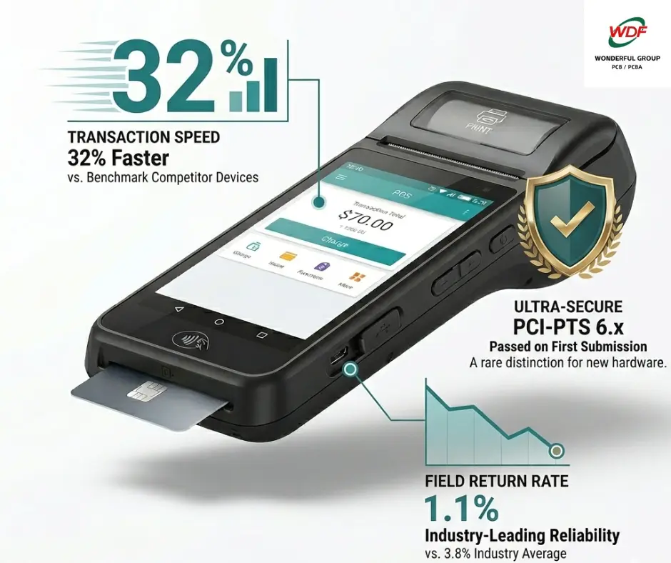
50,000 units. Three markets. PCI-PTS 6.x cleared on the first submission. That is where smart POS terminal project ended up — but the starting point was considerably messier.
WonderfulPCB was brought in as a full engineering partner, not just a board house. The scope covered everything: market research, industrial design, hardware architecture, PCB design, DFM optimization, reliability testing, and mass production ramp. The product? A handheld Android POS terminal with a 5.5-inch touchscreen, 58mm thermal printer, EMV chip and NFC card reader, 5,200mAh battery, and IP54 protection — all in a chassis under 380 grams.
The client was a fintech company deploying to street-level retailers and restaurant staff in Southeast Asia, South Asia, and Sub-Saharan Africa. Their ask was simple in concept: build something that works all day, survives being dropped, processes payments securely, and does not cost a fortune. What that actually meant in engineering terms took 14 months to figure out.
| Key Outcomes • First batch: 50,000 units shipped on schedule • Transaction speed: 32% faster than benchmark competitor devices • PCI-PTS 6.x: passed on first submission (rare for a first-time device) • Field return rate: 1.1% vs. 3.8% industry average • BOM cost: 17% below initial design estimate after DFM • Thermal printer head: validated at 80km life — beating the 50km requirement |
2. What Was Actually Wrong with Existing Devices
Before touching a schematic, the team spent time in the field. Real retail environments. Real operators. Seven competing POS terminals were purchased, torn down, and handed to actual merchant staff for two-week trials. The feedback was consistent — and damning.
Who Was Using These Things
The end users were not office workers. They were restaurant staff moving between tables, market vendors operating outdoors under direct sun, and delivery agents running on 4G because fixed broadband was either unavailable or unreliable. What they shared was zero tolerance for a device that slowed them down or died mid-shift.
The Real Problems
• Batteries gave out before the shift did. Most competitor devices shipped 3,000–3,600mAh cells and throttled badly with LTE and the printer running together. By hour six, operators were hunting for wall sockets.
• Screen visibility outdoors was poor. Display brightness topped out around 400 nits on most devices tested — borderline unreadable in sunlit conditions. Mobile vendors complained about this constantly.
• NFC was unreliable. On three of the seven devices, contactless payment failed at least once every ten attempts. The root cause, as the teardowns revealed, was antenna placement near metallic shielding. Nobody had fixed it.
• Durability was an illusion. Single-wall plastic chassis, minimal internal bracing, fragile port reinforcements. Most units showed structural wear within six months of daily use.
• Security certifications were outdated or absent. PCI-PTS 6.x had been the standard for a while, yet several devices were still running on older certifications — a real liability for acquiring banks.
The premium devices from the big names were properly engineered but priced out of the SME market entirely. The budget devices filled the gap in name only. WonderfulPCB’s position was clear: build something that belongs in the premium engineering bracket but lands at a mid-market price. Not a compromise device. A properly designed one.
3. Industrial Design — What Smart POS Terminal Needed to Feel Like
The design brief could be summarized in one sentence: it should disappear in your hand. The operator should never be thinking about the device — only about the transaction.
The Form Factor Decisions That Actually Mattered
Eleven concept directions were generated. Three rounds of stakeholder review and foam mockup testing later, the team had a clear direction: gently radiused corners, a pronounced palm grip zone on the lower rear, and a screen tilted 12 degrees forward from vertical.
Why 12 degrees specifically? Empirical testing. At that angle, glare from overhead fluorescent lighting — the dominant light source in retail and restaurant environments — dropped by roughly 40% compared to a flat-face design. The screen remained fully readable from the customer side of the counter. Anything steeper started limiting the operator’s viewing angle. Anything less left the glare problem unsolved.
The printer sat at the top of the device with a rear-exit paper slot and a spring-loaded cover. During prototype testing, one observation changed the cover mechanism entirely: operators naturally rested the device on a surface when tearing a receipt. So the paper cover was redesigned for single-hand loading while the device sat flat. A small thing. Saved real time during peak hours.
The NFC Tap Zone — a Detail That Kept Getting Underestimated
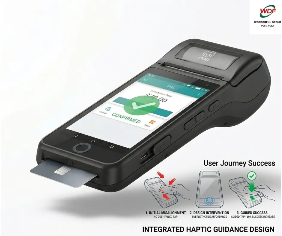
Most smart POS terminal devices in the tested lineup had an unmarked NFC zone. Customers would tap in slightly the wrong area, nothing would happen, and the operator would have to intervene. Testing on early prototypes showed that a subtle embossed ring on the front face below the screen reduced failed tap attempts by over 60%. Just a physical cue. No software involved.
CMF — Materials and Finish
The outer chassis used a PC/ABS blend with a soft-touch matte coating on grip surfaces and semi-gloss on the front face. Matte texture served two purposes: grip security when the operator’s hands were damp or greasy (very common in food service), and concealment of minor surface scratches that accumulate fast in daily commercial use.
The primary colorway — Midnight Slate — was validated through a merchant survey where 84% rated it as ‘professional and trustworthy’ versus the bright white or primary-color schemes common in budget devices. A secondary Arctic White was developed for hospitality clients.
4. Hardware for Smart POS Terminal
Choosing the Right Processor
Six SoC platforms were evaluated over three weeks. The selection came down to three weighted factors: hardware-accelerated cryptography (non-negotiable for PCI compliance), power efficiency under sustained multi-core load, and the depth of the vendor’s Board Support Package for firmware bring-up.
The Qualcomm Snapdragon QM215 won. Quad-core Cortex-A53 at 1.3GHz, Adreno 308 GPU, and — most importantly — hardware AES-256 and SHA-256 acceleration engines built in. In a benchmark running 200 consecutive EMV chip transactions, it sustained full performance with no thermal throttling. Three of the six evaluated competitors throttled noticeably under the same test.
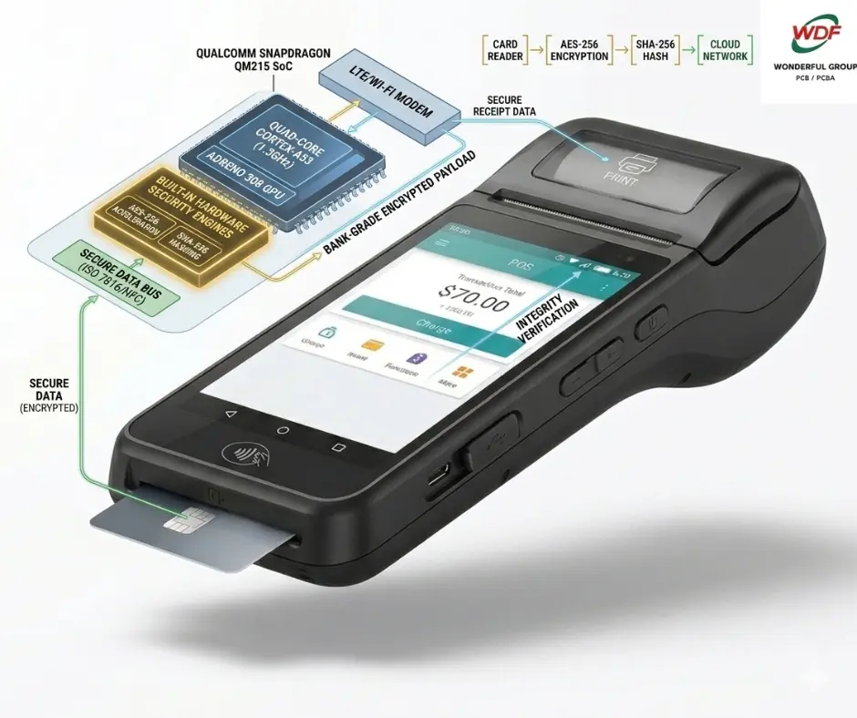
2GB LPDDR3 RAM and 16GB eMMC 5.1 completed the compute stack. Modest by smartphone standards, but this was a payment terminal. Sized for the job, not oversized for marketing purposes.
Security Architecture — Built In, Not Bolted On
PCI-PTS 6.x compliance is not a software feature you add at the end. It shapes the entire hardware design from day one. The security subsystem ran on a dedicated Security Controller IC, completely separate from the application processor. The Android OS had no view into this chip’s operations — by architecture, not by policy.
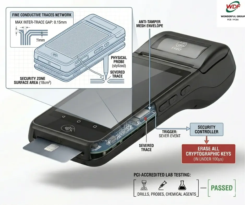
The anti-tamper mesh was one of the most demanding PCB layout tasks of smart POS terminal. A network of fine conductive traces had to cover the entire 18cm2 security zone with a maximum inter-trace gap of 0.15mm. Any physical probe inserted between those traces would sever at least one — triggering the Security Controller to erase all cryptographic keys in under 100 microseconds. That mechanism was tested in a PCI-accredited lab using probes, drills, and chemical agents. It passed every time.
ARM TrustZone handled the application-layer boundary. Payment processes — NFC token handling, EMV kernel execution, card data processing — ran exclusively inside the Trusted Execution Environment, isolated from anything happening in Android. A malicious app installed on the Android side? It would have no path to the payment data, regardless of what permissions it claimed.
NFC Antenna — the Problem Nobody Saw Coming
The original NFC antenna was a rectangular single-turn loop printed on the main PCB. Lab testing showed poor detection performance. Near-field scanning identified the cause: the printer motor’s ferromagnetic core was inducing eddy currents in the antenna loop, reducing effective field strength by around 35%.
The fix combined two changes. The antenna was moved to a flexible PCB laminated to the inner face of the front chassis cover — physically away from the main board’s interference environment. A custom ferrite sheet was bonded behind it, directing the magnetic flux forward toward the tap zone. After those changes, average detection range hit 4.2cm, clearing the 4cm requirement with room to spare.
Thermal Management
The QM215 SoC has a maximum junction temperature of 85 degrees C. The thermal printer head reaches 70–80 degrees C during sustained printing. Both running simultaneously — which is the normal scenario in a busy restaurant — required careful planning.
Finite element thermal simulation identified a heat buildup zone at the upper-center of the chassis interior where both heat sources overlapped under worst-case conditions. The solution used three components: a graphite thermal spreader bonded to the SoC package, a thermally conductive elastomer pad coupling that spreader to the chassis wall (using the chassis as a passive heatsink), and a low-conductivity polymer bracket isolating the printer from the SoC thermal zone. Under worst-case loading, SoC junction temperature stayed below 72 degrees C — a 13-degree margin against the limit.
5. Three Engineering Problems Worth Talking About
The Battery-Thickness Problem
The industrial design spec set a maximum grip-zone thickness of 22mm. The power budget for a full 8-hour shift demanded at least 5,000mAh. A standard 5,000mAh pouch cell would have pushed the device to 26mm. Four millimeters does not sound like much — but in a handheld device used for eight straight hours, those four millimeters are the difference between comfortable and fatiguing.
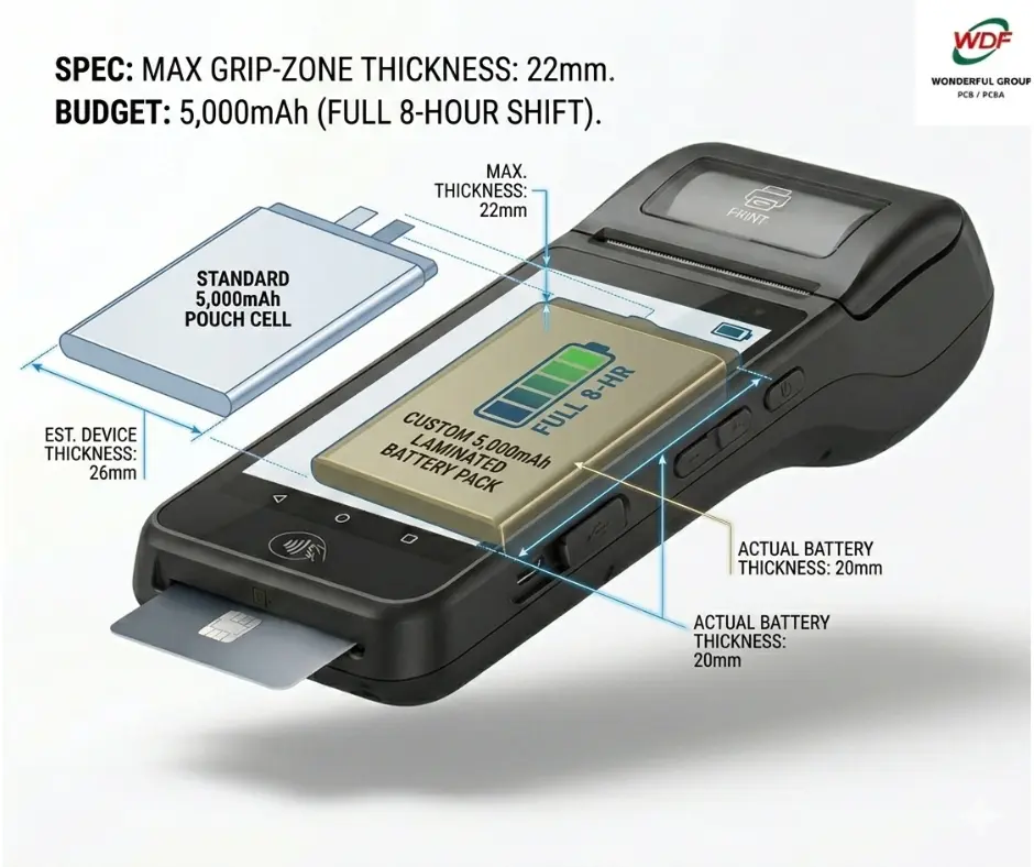
Three things had to happen simultaneously to close that gap. Twelve mid-density components on the main board were moved to 0201 and 01005 package sizes, recovering roughly 4cm2 of board area for the battery tray. A custom pouch cell was developed with a wider, flatter geometry than standard — reaching 5,200mAh at just 4.9mm thick. And the PCB stack-up was redesigned from 6 to 8 layers, shrinking the board footprint by 8% and freeing additional internal volume. No single change was enough. All three together were.
The Anti-Tamper Mesh vs. Signal Integrity
Routing the PCI-required security mesh — fine conductive traces at 0.15mm maximum spacing across 18cm2 — on a PCB that also carried high-speed digital signals and RF connections created a real problem. The mesh acted as an unintentional EMI coupling surface and degraded both NFC antenna performance and secure IC communication lines on early layouts.
The resolution was a dedicated PCB layer reserved exclusively for the mesh, separated from signal layers by solid reference planes on layers 4 and 6. The mesh was routed as a serpentine pattern rather than a grid, cutting capacitive coupling to adjacent layers by roughly 40% while maintaining the physical coverage density required by PCI. Signal integrity simulations were re-run after every revision until all metrics cleared simultaneously.
The Printer Vibration Problem
During the first functional smart POS terminal prototype build, operators described the feel of printing as ‘cheap’ and ‘alarming.’ The thermal printer’s stepper motor was generating a characteristic vibration at approximately 145Hz — right at the edge of the resonant frequency of the NFC antenna’s flexible PCB substrate. Dynamic analysis confirmed resonance coupling between 140Hz and 160Hz. Left unaddressed, that coupling risked intermittent NFC failures in the field.
A custom silicone vibration-damping mount was designed for the printer assembly, iterated through five physical prototypes. Each version was measured on an accelerometer-instrumented device. The final geometry achieved 78% vibration isolation at 145Hz — below the operator’s tactile perception threshold, and far enough from the NFC flex substrate to end the resonance coupling entirely.
6. Smart POS Terminal Manufacturing & Quality Control
Prototyping in Four Stages
The project moved through four defined prototype stages, each with entry and exit criteria. No stage could be skipped. That structure is what let the team catch the NFC interference issue and the printer resonance during EVT — rather than after tooling investment.
Appearance Models used SLA 3D printing to validate ergonomics and CMF before any tooling spend. Operator feedback at this stage moved the power button 3mm upward and increased the grip curvature radius by 1.5mm. Engineering Validation Test (EVT) used CNC-machined enclosures and hand-built boards — electrically functional but not production-representative. Design Validation Test (DVT) used first-shot injection molding and production PCBs. All three certifications — EMV L1, L2, and PCI-PTS 6.x — were submitted on DVT units and passed without a second submission. Production Validation Test (PVT) built 500 units on the full production line, distributed to beta merchants for 45 days. No issues that blocked mass production.
DFM — What Actually Changed
The original EVT design used seven wire harnesses to connect the main PCB to everything else: display, touchscreen, printer, NFC, camera, card reader. Assembly of those harnesses accounted for 23% of manual cycle time and was the top source of assembly defects — misrouted wires, pinched conductors, wrong connector seating.
Five of the seven were replaced with flexible printed circuits and ZIF connectors. The two that remained (battery and NFC antenna) needed controlled-impedance geometries that a standard FPC could not achieve. That change cut internal assembly cycle time by 31% and reduced cable-related defects by 88%, measured across the PVT build versus EVT. Screw count dropped from 14 to 9 through snap-fit features on the battery cover and printer door.
Reliability Testing Results
| Test | Result / Requirement |
| Drop — 1.5m, 6 faces | Zero PCBA or screen failures across 30 test units on reinforced concrete |
| Touchscreen tap life | 1,000,000 taps at 500g force — touch sensitivity within 2% of baseline |
| Thermal printer head | 80km paper validated — exceeds the 50km minimum requirement |
| ESD — contact/air | +/-8kV contact, +/-15kV air per IEC 61000-4-2 — no resets or data errors |
| Tumble — 300+ rounds | 0.5m equivalent rotating drum — no functional failures, cosmetic wear within spec |
| Climate | -10C to +50C operational — no battery swelling, no screen fogging |
| IP54 | Dust and water splash per IEC 60529 — zero ingress on PCBA post-test |
7. Final Product Specifications
| Processor | Qualcomm Snapdragon QM215, Quad-Core 1.3GHz Cortex-A53 |
| Memory | 2GB LPDDR3 RAM / 16GB eMMC 5.1 |
| Display | 5.5-inch IPS LCD, 600 nit, 1280×720, Optical Bonding |
| Printer | 58mm Thermal, 80mm/s, 80km head life validated |
| Battery | 5,200mAh Custom Pouch, 18W Fast Charge, 8hr+ operational |
| Security | Dedicated Security Controller, Anti-Tamper Mesh, ARM TrustZone TEE |
| Payment | Magnetic Stripe, EMV Chip L1+L2, NFC Contactless L1, QR Scan |
| Cellular | 4G LTE Cat-4 + Cat-M1/NB-IoT |
| Wi-Fi / BT | 802.11ac Wi-Fi 5, 2×2 MIMO / Bluetooth 5.0 + BLE |
| OS | Android 11, GMS Certified, TrustZone TEE |
| Dimensions | 180 x 76 x 22mm (grip zone), 378g with battery |
| Protection | IP54, 1.5m drop validated, IK08 |
| Certifications | PCI-PTS 6.x, EMV L1+L2, GMS, FCC, CE, RoHS 3.0 |
8. What Happened After Deployment
The first 90 days of field data of smart POS terminal told the real story. Transaction approval rates averaged 99.2% across all payment methods — the industry benchmark for the device class is around 97.4%. That 1.8-point difference, small as it sounds, translated directly into fewer failed checkouts, less friction for merchants, and measurable revenue protection for the client’s deploying partners.
Field return rates came in at 1.1% versus the 3.8% industry average. The client attributed that directly to the IP54 protection and the drop-resistance work — the two failure modes that had dominated their warranty queues with previous hardware. The 28% drop in field service calls within those first 90 days was not a surprise to the engineering team. It was the expected outcome of making durability a design constraint rather than an afterthought.
Merchant operator satisfaction scored 4.6 out of 5.0. The three highest-rated attributes: battery life, screen readability, and print speed. All three were precisely the pain points the research had flagged before a single line of schematic was drawn. That alignment between the original problem statement and the final user feedback is as close to validation as an engineering team can get.
What Comes Next
The platform was designed with future iterations in mind. There is an unpopulated footprint on the PCB for a secondary Secure Element, reserved for host card emulation and transit payment applications — no board redesign needed when that feature is required. The QM215 supports on-device ML inference, which is currently unused but available for future edge fraud detection or camera-based inventory recognition.
A biometric variant is already in DVT. The printer module is being swapped for a combined fingerprint sensor and compact receipt printer assembly. The chassis, PCB architecture, certifications, and production process from the first generation all carry forward. That is what modular design actually means in practice.
9. Conclusion
What made this project work was not any single engineering breakthrough. It was the decision to treat security, durability, ergonomics, and manufacturability as simultaneous constraints from day one — not as a sequential checklist where each team hands off to the next.
The battery-thickness problem required mechanical, electronic, and component engineering to move at the same time. The anti-tamper mesh required PCB layout and signal integrity to work as one problem, not two. The printer vibration was a mechanical issue that had RF consequences. Every hard problem in this project crossed discipline boundaries. The team was structured to work across those boundaries rather than hand over the fence.
50,000 units in the field. A 1.1% return rate. PCI-PTS 6.x on the first attempt. Those outcomes do not come from adequate engineering. They come from an engineering process that is honest about tradeoffs early, disciplined about validation, and genuinely integrated across every function that shapes the final product.
WonderfulPCB — Engineering the Future of Payment Hardware