You spend weeks manually tracing printed circuit board layouts. Artificial intelligence can do it in hours or in less time. Manual PCB reverse engineering is time-consuming, error-prone, and needs expert skills. AI and machine learning automate schematic generation, component detection, and trace routing analysis. You reduce time by 70%, improve accuracy to 90-95%, and lower costs significantly.
This guide demonstrates how AI powered PCB automates PCB reverse engineering. You will learn which machine learning techniques work best, when to use AI versus manual methods, and how to implement AI tools in your workflow.
What is AI-Powered PCB Reverse Engineering?
You use artificial intelligence to automatically evaluate PCB images and generate complete schematics. Machine learning algorithms discover components, identify traces, locate vias, and map electrical connections without manual interference. Neural networks trained on millions of PCB layouts identify patterns and process high-resolution photographs or scans of your PCB. Traditional reverse engineering depends on manual tracing with multimeters and visual inspection. A complex 8-layer board takes several weeks. AI transforms this, like you picture the printed circuit board, upload images, and get draft schematics within hours. AI handles pattern recognition while you focus on validation and complex analysis.
This automated method holds PCBs with hundreds or thousands of components. You get results in hours that would take weeks manually. The AI maintains consistent accuracy across the entire board without the fatigue that affects human engineers during repetitive tasks.
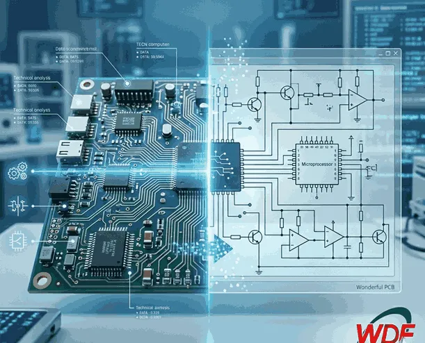
Figure 1 Manual PCB reverse engineering (left) versus AI-powered automated analysis (right)
How AI Changes Traditional Reverse Engineering
Traditional PCB reverse engineering relies completely on manual work. You trace each connection with a multimeter, visually inspect component markings through a magnifying glass, and hand-draw schematic symbols. A complex 8-layer board with 500 components can take 3-4 weeks of continuous work. Chances of error are more. Components with worn markings need vast research to identify.
Artificial intelligence powered reverse engineering changes this process completely. You photograph both sides of the PCB with a good camera or scanner. Upload the images to the AI system. The software processes everything automatically component detection, trace routing, via identification, and connection mapping. Within hours, you have a draft schematic ready for review. Your engineering time shifts from repetitive tracing to intelligent validation and refinement.
The key difference shows how you utilize your time. AI handles pattern recognition tasks where it excels identifying thousands of similar components, following parallel traces, mapping regular grid patterns.
Machine Learning Techniques Used in PCB Reverse Engineering
Convolutional Neural Networks (CNNs) detect and organize components. These networks process images through layers that recognize edges, shapes, and finally component types. Image segmentation separates components from traces. Object detection locates thousands of parts automatically with confidence scores. OCR reads component labels and part numbers, even small or rotated text, then cross-references databases for full specifications.
Neural networks follow copper traces across multilayer boards using specialized algorithms. Graph neural networks map connections between components. Via detection identifies connection points between layers. Advanced algorithms reconstruct signal paths even with incomplete visual data using context clues and typical routing patterns.
AI converts physical layout to logical schematics through netlist creation and functional grouping. Rule-based systems apply engineering principles. Machine learning predicts circuit functionality based on component arrangement. Output formats work with Eagle, Altium, KiCad, and other CAD tools.
AI-Powered PCB Reverse Engineering vs Manual Methods
You need to select the right reverse engineering method for your project. The comparison between AI-powered and manual methods shows clear differences in time, cost, and capabilities. This table shows how each approach performs across critical factors:
The comparison reveals clear differences in time, cost, and capabilities:
| Factor | AI-Powered | Manual |
| Time | Hours to days | Weeks to months |
| Accuracy | 90-95% (validated) | 85-95% (expert dependent) |
| Cost | Lower (tool + validation) | Higher (labor intensive) |
| Best For | High-volume, standard PCBs | Custom, unusual designs |
Use AI powered PCB approach for high component density, tight deadlines, and standard designs. Use manual methods for unusual components, extremely damaged boards, or security-critical validation. The hybrid approach works best. AI handles 80-90% of work, manual validation covers the critical final 10-20%.
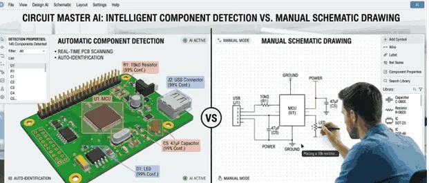
Figure 2 AI PCB reverse engineering software interface
When to Choose AI vs Manual
Use AI when you face high component density boards with hundreds of similar parts. AI excels at processing multiple similar boards quickly, making it ideal when you need to reverse engineer several units of the same product. Tight deadlines favor AI’s speed advantage. Standard consumer electronics, industrial controllers, and commercial equipment typically work well with AI analysis because they follow common design patterns the AI has learned.
Use manual methods when you encounter unusual components not in AI training databases custom ASICs, proprietary modules, or rare vintage parts. Extremely damaged boards where traces are broken or components missing need human problem-solving. Security critical validation for military or medical applications requires expert human verification. One-off custom designs with unconventional layouts challenge AI systems trained on typical patterns.
The hybrid approach combines both methods. Start with AI for the initial 80-90% of work. component detection, basic trace routing, and netlist generation. Then switch to manual validation for the final 10-20% verifying critical connections, resolving ambiguous traces, and checking unusual circuit sections. This hybrid roadmap carries the best balance of speed and accuracy for most projects.
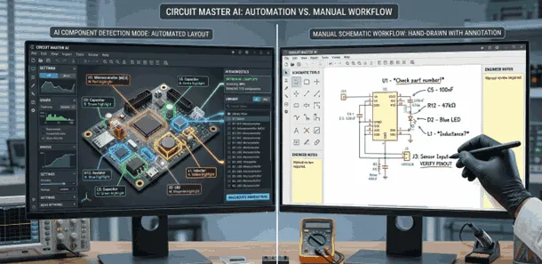
Figure 3 AI automated analysis versus traditional manual PCB tracing workflow
Top AI-Powered PCB Reverse Engineering Tools in 2026
Commercial Artificial intelligence platforms provide complete workflows from image capture to schematic export. These cloud-based solutions include trained neural networks and component libraries with millions of parts. Subscription pricing approximately ranges from $2,000 to $15,000 annually. Key features include 95%+ component detection accuracy, multiple export formats, and batch processing capabilities.
Open-source tools using TensorFlow and PyTorch are available on GitHub. These are free and customizable but require ML expertise, Python programming, and powerful GPUs. They suit researchers and companies with AI capabilities but not engineers needing quick results.
Wonderful PCB combines AI automation with expert validation. We use commercial AI for initial analysis, then engineers review every result. This hybrid approach delivers AI speed with 98%+ human-verified accuracy. We handle multilayer boards up to 12+ layers, complex designs, and provide complete deliverables in quick time.
How AI-Powered PCB Reverse Engineering Works: Step-by-Step
Step 1: PCB Image Acquisition
You start by photographing or scanning both sides of your printed circuit board at high resolution. Use at least 300 DPI for good results, though 600 DPI works better for dense boards. Good lighting prevents shadows and glare that confuse AI algorithms. Position the camera or scanner perpendicular to the board to minimize perspective distortion.
For multilayer boards, X-ray imaging captures internal layer structures invisible to cameras. X-ray systems reveal buried vias, internal traces, and layer stack-up details. Some AI platforms integrate with X-ray equipment, while others need you to provide X-ray images separately. Image pre-processing software then aligns multiple images, adjusts contrast for optimal component visibility, and minimize noise from scratches or substrate patterns.
Step 2: AI Component Detection
Neural networks process your PCB images to identify and classify every component. The AI draws bounding boxes around each resistor, capacitor, IC, connector, and other parts. It gives component types with confidence scores showing how certain the identification is. Components with low confidence scores get flagged for manual verification.
OCR engines read part numbers and markings visible on components. This automated reading works on text as small as 1mm height. The system rotates its reading to handle components placed at any angle. Detected part numbers get cross-referenced against electronic component databases to retrieve full specifications. The AI generates a complete bill of materials listing every component with manufacturer part numbers, values, package types, and quantities.
Step 3: Trace and Connection Analysis
AI follows copper traces across the PCB to map electrical connections. Trace detection algorithms track conductive paths from component pins through the board. They handle complex routing including curved traces, traces that narrow at vias, and traces partially obscured by solder mask. Via detection links layers in multilayer boards by identifying connection points between internal and external layers.
The system generates a netlist showing all component interconnections. Each net represents a unique electrical node with all pins connected to it. This connectivity information creates the foundation for schematic generation. The AI can differentiate between power traces, ground connections, and signal traces based on trace width, routing patterns, and connected components.
Step 4: Schematic Generation
AI converts the physical PCB layout into a logical schematic diagram. It identifies component symbols according to their function and arranges connections to minimize line crossings. Machine learning models predict circuit functionality based on component arrangement and connection patterns. A microcontroller with surrounding capacitors, crystal, and programming connector gets identified as a complete MCU circuit. This functional understanding helps organize the schematic logically. Output formats include Eagle XML, Altium files, KiCad projects, and OrCAD designs, plus neutral formats like EDIF for maximum compatibility.
Step 5: Human Validation and Refinement
An engineer reviews the AI-generated output for accuracy. This validation catches errors in the AI powered circuit board, misidentified components, missed connections, or incorrectly routed traces. Manual corrections address complex or ambiguous sections where AI confidence was low. The engineer verifies important connections using the original PCB, sometimes with multimeter continuity checks for important nets.
Final schematic verification ensures the circuit makes logical sense. Power supply voltages should be correct. Communication buses should have proper termination. Reset circuits should follow the microcontroller datasheet. This functional verification confirms the schematic represents a working circuit, not just accurate component connections. Complete documentation includes component datasheets, design notes explaining unusual circuits, and revision history.
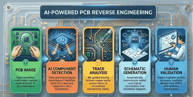
| Figure 4 Five-step AI PCB reverse engineering process |
Key Applications of AI PCB Reverse Engineering
Legacy system maintenance for equipment that survives manufacturer support. Production machinery, medical devices, and industrial controls often run 20-30 years. AI makes schematic recovery economically feasible. Outdated component replacement requires understanding circuits fully to recognize modern equivalents.
Quality control verifies manufactured PCBs that match design specifications. Fake detection compares suspect boards against authentic designs. IP protection documents design for patent applications. Product redesign modernizes legacy products with updated components. Educational purposes help students learn by analyzing professional designs.
Advantages and Limitations of AI PCB Reverse Engineering
Advantages: 70% faster than manual methods. Projects that took weeks now complete in days or even in hours. Reliable accuracy eliminates human fatigue errors. Handles 1000+ component boards efficiently. Scalable for multiple boards simultaneously. Cost-effective volume work with lower per-board costs. Reduces skill barrier so intermediate engineers can execute advanced analysis.
Limitations: Requires quality images as poor photos reduce accuracy of PCB design. Struggles with custom or unusual components. Initial tool costs $2,000-$15,000 annually. Training data dependency means AI works best on boards like training examples. Cannot infer firmware logic, hardware analysis only. Still needs human validation for critical applications.
Tip: Use AI for 80-90% automation, reserve 10-20% for manual review. This hybrid approach provides speed and accuracy.
Why Choose Wonderful PCB for AI-Assisted Reverse Engineering
We combine cutting-edge AI tools with experienced engineering validation. Our process uses AI for rapid analysis, then senior engineers verify every detail. You get guaranteed 98%+ schematic accuracy with AI speed and human precision. We validate circuit functionality, not just connections.
Our services handle simple 2-layer to complex 12-layer boards, flexible circuits, and rigid-flex designs. We offer IC decryption and firmware extraction for complete system understanding. PCB cloning and redesign capabilities take you from reverse engineering to production. X-ray imaging reveals internal layers in multilayer boards.
With 30+ years of experience across all industries, we guarantee confidentiality and IP protection. Standard turnaround is 5-10 days. We provide end-to-end support from reverse engineering through manufacturing, BOM sourcing, assembly, and testing.
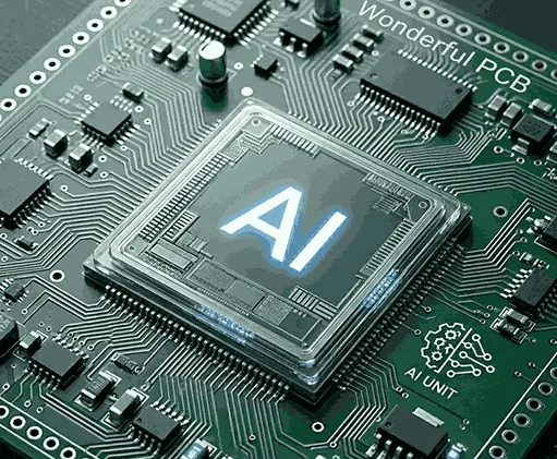
Figure 5 Wonderful PCB Professional PCB Reverse Engineering
Frequently Asked Questions
How accurate is AI-powered PCB reverse engineering compared to manual methods?
AI achieves 90-95% accuracy for component detection and trace routing. With expert validation, final accuracy exceeds 98%. Manual methods reach 85-95% but take much longer time. The combination of AI automation plus human review delivers the best results.
Can AI reverse engineer multilayer PCBs with internal layers?
Yes, when combined with X-ray imaging. X-rays reveal internal traces and vias. AI processes X-ray images with surface photographs to generate complete schematics for boards up to 12+ layers. Without X-ray, AI can only analyze visible surface layers.
How long does AI PCB reverse engineering take?
Simple 2-layer boards take about 1 day total. Complex 8-layer boards require 5-7 days. This is 70% faster than manual-only methods. Time depends on board complexity, component count, and whether multilayer X-ray imaging is needed.
What image quality do I need for AI PCB analysis?
Minimum 300 DPI resolution, though 600 DPI works better for dense circuit boards. Use good lighting without glare.
Is it legal to use AI for PCB reverse engineering?
Reverse engineering is legal for devices and project you own, for learning, repair, or interoperability. However, copying designs for commercial purposes may violate patents or copyrights. Always consult legal counsel for your specific situation.
Conclusion
AI transforms PCB into reverse engineering from weeks to days with 70%-time savings and improved accuracy. Machine learning handles repetitive tasks while you focus on complex analysis. The hybrid approach combining AI automation with human validation delivers both speed and accuracy. sAI tools become more accessible by improving accuracy and decreasing costs. AI-powered reverse engineering will become as common as CAD design tools today.