Your next project requires a 10-layer PCB, but you are thinking how manufacturers actually fabricate complex boards. Wonderful PCB gives you information about stackup design, material selection, fabrication steps, and how to pick the right 10 layer pcb stack up factory for your needs.
Fundamentals of 10-Layer PCB Technology
Multilayer PCB Overview
Multilayer boards stack copper and insulating material into a sandwich. Two layers? Simple. Four layers? Still manageable.
But ten layers?
Now you enter territory where precision matters at every step. Each added layer brings more routing space. Better shielding. Improved power distribution. Yet complexity grows fast. The alignment between layers must be within microns; otherwise, your board fails.
10-Layer PCB vs. Other Multilayer Boards
Why choose ten layers instead of eight or twelve?
Six-layer boards work well for moderate-density designs, but they run out of room as signal counts increase. Eight layers help, though power integrity sometimes suffers. Twelve layers? Overkill for most applications, plus the costs jump.
Ten layers hit a sweet spot. You gain four signal layers, two ground planes, two power planes, and two outer routing layers. That balance works for high-speed digital circuits, RF modules, and dense part layouts without breaking your budget.
Compare this to a four-layer board where you constantly fight routing congestion. The 10-layer PCB stackup provides breathing room exactly where you need it.
Standard Stack-Up Configurations and Material Layers
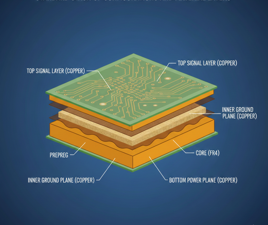
Signal Layers
Signal layers carry your traces, data lines, clocks, and address buses. In a ten-layer configuration, signal routing occurs on layers 1, 3, 4, 6, 7, and 10.
Outer layers handle low-speed signals. Inner layers work better for high-speed differential pairs because they sit between reference planes.
Some designers place slow signals outside and fast signals inside. Others mix them based on trace length requirements. There is no single correct approach. Your application decides the priority.
Power and Ground Planes
Layers 2 and 9 are often used as ground planes. Layers 5 and 8 serve as power planes, though you can split layer 5 into multiple voltage domains.
Ground planes should stay solid whenever possible.
Splitting the ground creates return-path problems that degrade signal integrity. Power planes can split, but do it carefully. Traces crossing split boundaries see impedance discontinuities.
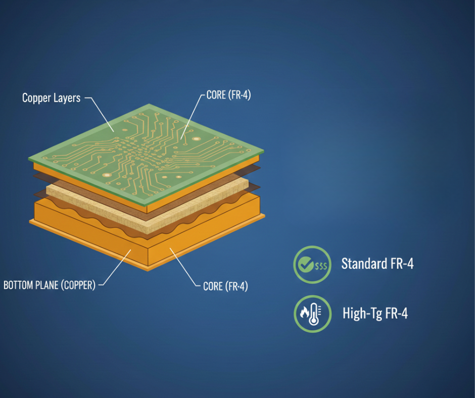
Dielectric and Core Materials
FR-4 remains the workhorse material for most 10 layer PCB manufacturing projects. Standard FR-4 costs less and performs well up to a few gigahertz. High-Tg FR-4 handles lead-free soldering temperatures without delaminating.
Need better high-frequency performance?
Rogers laminates bring lower loss tangent and stable dielectric constant across temperature swings. Polyimide survives extreme heat cycles. PTFE-based materials work for microwave frequencies but cost significantly more.
Prepreg sheets bond core layers together during lamination. Thickness varies—for example, 2116 prepreg measures about 4 mils, 7628 runs around 7 mils. Mix and match prepreg types to get your target 10 layer pcb thickness.
Design Considerations Unique to 10-Layer Structures
Impedance Control
Once signals exceed a few hundred megahertz, you will encounter impedance issues. It’s non-negotiable. Your first high-speed board can be disastrous if you ignore the dielectric constant. Why? Trace width and copper weight aren’t just numbers; they’re the law.
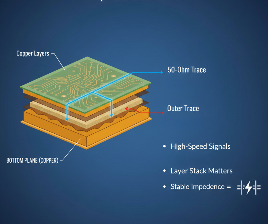
A ten-layer stackup lets you sandwich signals between planes. So what? It makes 50-ohm traces actually work. Inner layers stay close to their reference, while outer ones are distant, lonely, and unpredictable.
That means you need wider traces on layers 1 and 10 to match the same impedance as narrower traces on layer 3 or 6.
Stackup calculators help, but always request impedance testing from your 10 layer pcb stack up manufacturer.
Signal Integrity
High-speed signals hate discontinuities.
Via stubs add capacitance. Layer transitions create reflections. Crosstalk between adjacent traces distorts waveforms. Ten layers give you options to mitigate these problems.
Return current flows in the plane directly beneath your signal trace. When a trace changes layers, the return current must find a path through vias or capacitors to the new reference plane.
Poor return paths cause EMI and ground bounce.
Place stitching vias near layer transitions to keep return current loops tight.
Power Distribution and Thermal Management
More layers mean better power distribution. Dedicated power planes lower DC resistance and spread current evenly.
But heat becomes a concern because copper conducts heat well, yet FR-4 insulates. Ten layers of material trap heat inside the board.
Thermal vias beneath hot components conduct heat to the outer layers, where air or heat sinks dissipate it. Size your power planes to handle current without excessive temperature rise.
10 Layer PCB Manufacturing Process
- Design and Prototyping
Start with the schematic. Why wait? Shift it into Altium or KiCad layout. Define that stackup early, or you’re dead. Export Gerbers, drills, and fab drawings—specify your copper weights and tolerances.
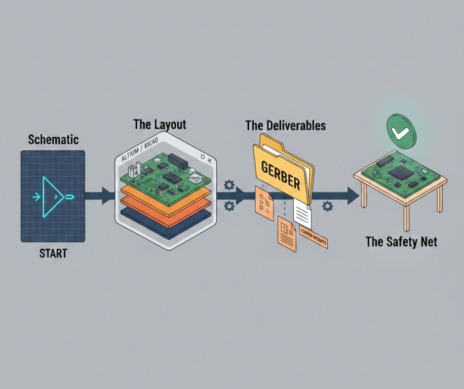
Build a prototype first. Catch the mess now. If you wait for full production, the cost of a tiny error will haunt your bank account.
- Material Preparation and Selection
Manufacturers stock core laminates and prepreg rolls. They cut sheets to panel size. For a ten-layer board, you need multiple core layers plus prepreg sheets to bond them.
Material selection affects performance and price.
Standard FR-4 works for most digital designs. High-frequency circuits need low-loss laminates. High-current applications demand thicker copper.
- Inner Layer Fabrication
Inner layers get patterned before lamination. The process starts with a copper-clad core. A layer of photoresist coats the copper.
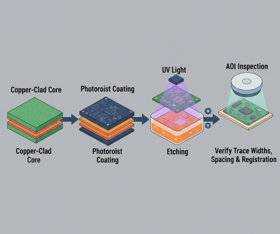
UV light exposes the resist through a film or laser direct imaging. Developing removes unexposed resist, leaving bare copper in unwanted areas. Etching dissolves that copper.
Each layer gets inspected under AOI to verify trace widths, spacing, and registration marks.
- Layer Alignment and Registration
Registration marks, small targets etched into each layer, help align cores and prepreg during stacking. Misalignment by more than a few mils causes vias to miss pads or traces to short against planes.
Some 10 layer pcb stack up factories use pin lamination, where tooling pins pierce all layers to hold alignment. Others rely on vision systems alone.
Tolerance requirements tighten as via sizes shrink, microvias demand alignment within ±2 mils or better.
- Lamination Process
Stacking happens in a clean room. Layers go into a press in sequence. Vacuum removes air pockets.
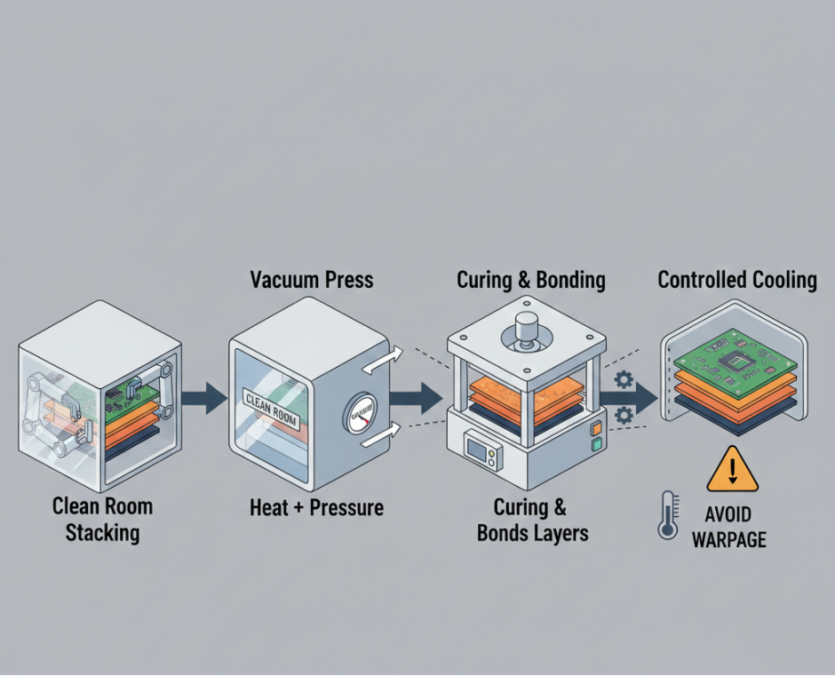
Heat and pressure cure the prepreg resin, bonding everything into a solid panel.
Cooling must happen slowly to avoid warpage. Uneven cooling creates internal stress that bows the board.
- Drilling Operations
After lamination, you have a blank multilayer panel. Now drill holes for vias and component leads.
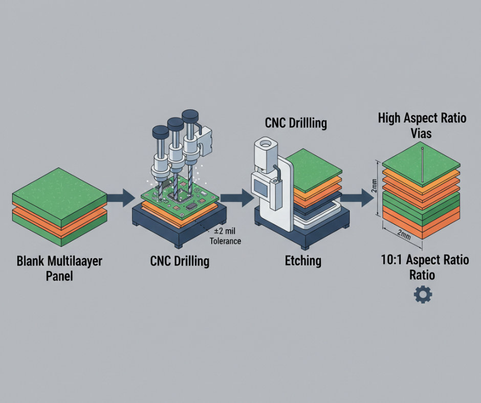
CNC drilling machines use carbide or diamond-coated bits. Hole diameter tolerances run ±2 mils for through-holes, tighter for microvias.
High aspect ratio holes challenge plating processes. A ten-layer board at 2mm thickness with 0.2mm vias has a 10:1 aspect ratio, right at the edge of standard capability.
- Plating and Copper Deposition
Bare epoxy walls are useless until electroless copper deposition adds a conductive skin. Then, electroplating builds it to 25 microns. Why? It’s the electrical bridge between layers. If the centre is thin, thermal stress can cause the via to crack. Uniformity is life.
- Circuit Pattern Imaging and Etching
Outer layers get patterned post-plating. Dry film resist, masks, and etching—just like the inner layers. Why? Precision. Fine-pitch traces demand tight control, or the signal disappears into copper soup.
- Solder Mask Application
Solder mask is usually green, though other colors are available to coat the outer layers, leaving pads and vias exposed.
Liquid photoimageable solder mask is applied in thin layers, exposed to UV light, and developed. It protects copper from oxidation and stops solder bridges during assembly.
- Surface Finishing
Bare copper oxidizes quickly. Surface finishes protect pads until assembly.
HASL dips the board in molten solder, which is cheap but uneven. ENIG plates nickel, then gold over pads, flat, suitable for fine-pitch parts, but more expensive.
Your choice depends on the assembly process and storage time. ENIG is suitable for most 10-layer PCB manufacturing projects, especially when wire bonding or long shelf life is required.
- Electrical Testing
Every board must pass electrical testing.
Flying probe testers use moving needles—great for prototypes. But for big runs? Fixture-based testers with pins are faster, though that custom fixture isn’t free. Why guess if it works? A Time-Domain Reflectometer shoots signals down the line to verify your 50-ohm traces actually meet spec. Precision matters.
- Final Inspection and Quality Control
Visual checks catch the ugly stuff—scratches or solder mask voids—but why stop there? Dimensional checks verify if the board actually fits the box. X-rays peek inside at vias, hunting for misalignment or hidden voids. ISO 9001 means they follow the rules, but IPC classes are the real boss. Class 2 accepts some minor flaws, while Class 3 demands perfection.
Important Manufacturing Considerations
Layer-to-Layer Registration Tolerance
Errors pile up fast. A 2-mil inner-layer shift plus 3 mils from lamination and 2 mils of drill wander? That’s 7 mils of chaos. Suddenly, your drill misses the pad entirely. Open circuit. Game over. Tight tolerances aren’t free because they require slower, fancier machines.
Aspect Ratio Management
This is just the hole depth divided by the diameter. A 1.6mm board with 0.2mm vias is an 8:1 ratio. As that number climbs, plating quality dives. Above 12:1? You’re begging for thin copper or voids in the centre. Use pulse plating or blind vias to cheat the depth.
Via Hole Quality and Reliability
Vias die when plating cracks under thermal stress. Copper and epoxy expand at different rates—they fight each other. IPC-6012 sets the rules for plating thickness. If reliability is your soul, demand microsection reports from your factory.
Materials Used in 10 Layer PCB Manufacturing
FR-4 Standard Grade
It’s the cheap, glass-epoxy classic. Why use anything else for basic stuff? With a near 130°C, it softens if things get too hot. The dielectric constant hovers around 4.4, but it shifts with frequency.
High-Tg FR-4 Materials
Pushing Tg to 180°C changes the game for lead-free reflow. It survives thermal cycling, a common feature of cheaper boards. Automotive and industrial gear love this stuff because it simply refuses to quit under heat.
Rogers High-Frequency Laminates
For RF or 10 Gbps+ speeds, standard FR-4 is too leaky. Rogers offers tight and low loss. Pro tip: Use a hybrid stackup—Rogers for high-speed traces, FR-4 for the rest. Why pay for a full Rogers board?
Polyimide for High Temperature
This is the aerospace, surviving 260°C. It’s flexible and handles thermal expansion like a champ. The catch? It costs five times as much as FR-4. Lead times stretch because not every factory keeps this expensive gold in stock.
Copper Foil Thickness Options
Weight is measured in ounces. 1 oz is 35 microns. Half-ounce is standard for signals, but power planes need 1 or 2 oz. Thicker copper handles current, but makes etching fine lines a nightmare. It’s a trade-off.
Heavy Copper for High-Current Layers
Got 10 amps? Go heavy. It kills heat and resistive loss, but beware the “undercut” during etching where sidewalls slope. It also bloats your 10-layer thickness budget. Plan or your board won’t fit the connector.
Design Considerations and Guidelines
Stackup Design Best Practices
Symmetric Layer Arrangement
A balanced stackup has mirrored layer pairs around the center. This symmetry keeps the board flat during lamination and reduces warpage during soldering.
Asymmetric stackups bow the board because copper expands differently than FR-4.
Ground and Power Plane Positioning
Place ground planes as close to outer layers as possible. This reduces EMI and provides a low-impedance return path for signals on layers 1 and 10.
Power planes should sit between signal layers to decouple high-frequency noise.
Splitting ground planes is usually a bad idea. Signals crossing a split see discontinuous return paths, causing radiated emissions and crosstalk.
Controlled Impedance Requirements
High-speed signals need transmission line behavior. That means controlled impedance is usually 50 ohms single-ended or 100 ohms differential.
Impedance depends on trace width, thickness, distance to reference plane, and Dk.
Use an impedance calculator during stackup design. Then, verify with impedance testing after fabrication. Most 10 layer pcb stack up manufacturers charge extra for impedance control, but it is worth it for gigabit designs.
Via Technology
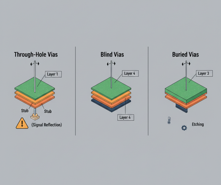
Through-Hole Vias
Through-hole vias drill from layer 1 to layer 10, connecting all layers. They are cheap, reliable, and easy to inspect.
Downside: they consume space and create stubs below the lowest connection point. Stubs act as antennas, reflecting high-frequency signals.
Blind Vias
Blind vias connect an outer layer to an inner layer but do not go all the way through. Example: layer 1 to layer 4.
They save space and eliminate stubs.
But they cost more because they require multiple drilling and plating steps.
Buried Vias
Buried vias connect two inner layers without reaching the outer layers. These are formed before final lamination, which adds process complexity.
Buried vias are common in HDI boards but rare in standard ten-layer designs unless routing is extremely tight.
Thermal Management
Thermal Via Placement
Power parts, voltage regulators, FPGAs, and RF amplifiers generate heat. Thermal vias beneath these parts conduct heat from the top layer through the board to a ground plane or a bottom-layer heat spreader.
Array 20-50 small vias under the component thermal pad. More vias lower thermal resistance.
Heat Dissipation Strategies
Thick copper planes dissipate heat better than thin traces. Use 2 oz copper on power planes if thermal load is high.
Add thermal reliefs on power planes to ease soldering, though thermal reliefs increase thermal resistance.
Airflow helps. If your enclosure has fans, orient the board to maximize air flow over hot parts.
Signal Integrity Considerations
High-Speed Signal Routing
Signals above 1 Gbps need careful routing.
Keep traces short. Avoid stubs. Match lengths for differential pairs and multi-bit buses. Route high-speed signals on inner layers when possible; stripline has better shielding than microstrip.
Differential Pair Routing
USB, HDMI, PCIe, and Ethernet all use differential pairs. Two traces carry opposite signals.
For this to work, traces must be tightly coupled and length-matched.
Most pairs target 100 ohms differential. Route pairs together do not separate them. Avoid vias in the middle of a pair.
Choosing Wonderful PCB Manufacturer
You have finalized your 10 layer pcb stackup design. Now you need a factory to build it.
How do you pick?
Price matters, but so does quality, lead time, and support.
Manufacturing Capabilities and Capacity
Can the factory handle ten layers? Ask about maximum layer count, minimum trace width, minimum hole size, and aspect ratio limits.
If your design pushes boundaries 3-mil traces, 6-mil vias, 12:1 aspect ratio, you need a manufacturer with advanced equipment.
Capacity affects lead time. A factory running at full capacity can quote six weeks. One with spare capacity might give in three.
Experience with Complex Multilayer Boards
Years in business do not guarantee multilayer expertise.
Ask for 10 layer pcb stackup examples, photos of finished boards, customer testimonials, or case studies. Request a factory tour if possible.
IPC certification shows the factory follows industry standards. ISO 9001 means documented quality processes. Match certifications to your industry.
Quality Certifications and Standards
IPC Class 2 applies to general electronics commercial products, where minor cosmetic flaws are acceptable. IPC Class 3 is high-reliability aerospace, medical, and military applications where defects cannot be tolerated.
Ask if the factory performs 100% electrical testing or sample testing. For important applications, 100% testing is worth the extra cost.
Lead Time and Delivery Performance
The standard lead time for a ten-layer board is 2-4 weeks. Quick-turn services cut that to 5-10 days but cost 50-100% more.
On-time delivery matters as much as the quoted lead time.
A factory that promises two weeks but ships in three disrupts your schedule. Check reviews or ask for delivery performance data.
Prototyping Services Availability
Prototyping and production differ. Prototypes are run in small quantities (1-10 boards) to verify designs. Production runs hundreds or thousands.
Prototype-focused shops respond fast, accept small orders, and tolerate design changes. But the per-board cost is high.
Ideally, find a 10-layer PCB stackup factory that can both prototype with them and scale to production without switching suppliers.
Technical Support and DFM Assistance
Design for manufacturability catches errors before fabrication.
A good manufacturer reviews your Gerber files and flags problems, such as traces that are too narrow, clearances that are too tight, and vias that are too small.
Technical support answers questions during design. What stackup should I use? Can you build 4-mil traces on 2 oz copper?
Responsive support accelerates your project.
Competitive Pricing
Price varies wildly. A ten-layer prototype cost $200-500 per board from a domestic quick-turn shop or $50-150 from an overseas factory.
Volume pricing drops 100 boards can run $20-40 each. Get 10 layer pcb stack up quotes from multiple suppliers to compare.
Beware low-ball quotes. If one factory quotes half the price of everyone else, ask why.
Minimum Order Quantities
Minimum order quantity sets the smallest number of boards you can order. Prototype shops often have an MOQ of 1-5 boards. Production factories will require 50, 100, or more.
If your application needs just a few boards, choose a low-MOQ 10-layer PCB stack-up manufacturer. For consumer products heading to mass production, a higher MOQ is not a problem.
Building a ten-layer board takes precision at every step from stackup design through final testing. You need the right materials, tight process control, and a manufacturer with proven multilayer experience. Understanding 10-layer PCB thickness and impedance control helps you design boards that work the first time.