Most engineers think adding layers to a PCB is just about cramming more traces into less space. Wrong. The jump from 2-layer to 4-layer boards changes how your entire circuit behaves electrically. You get dedicated planes that work as shields. This is more important than the $20 price difference between prototypes.
What is the Standard 4-Layer PCB Stack-up?
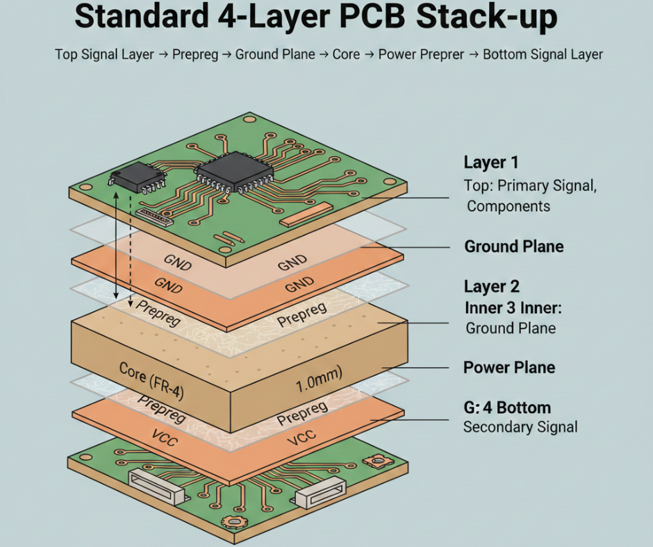
Here’s something nobody tells you up front: the layer stack in a 4-layer board isn’t random. You cannot just stack copper sheets however you want and expect good performance.
The standard construction follows this sandwich pattern:
Top Signal Layer → Prepreg → Ground Plane → Core → Power Plane → Prepreg → Bottom Signal Layer.
Layer 1Top
Your primary signal layer. Components sit here. Traces run here. This is where most of your routing happens because you need access to component pads.
Layer 2 Inner
Ground plane. This entire copper sheet connects to GND. Why dedicate a whole layer to ground? Because high-frequency signals need a solid return path sitting right underneath them. When a signal travels on Layer 1, the return current flows directly below it on Layer 2. This creates a small loop area, stopping EMI issues before they start.
You might have seen designs where engineers tried using a ground grid instead of a plane. Disaster. The signal integrity issues cost them three board revisions.
Layer 3 Inner
Power plane. Usually connects to your main VCC rail, whether that is 3.3V, 5V, or 12V, depending on your design. This plane distributes power across the board with minimal impedance. You get a stable voltage at every IC without fat power traces finishing routing space. Some designs split this layer between multiple voltages, like 3.3V and 5V. Works fine if you keep proper clearance between the splits.
Layer 4 Bottom
Secondary signal layer. You route here when Layer 1 fills up or when you need to escape BGA fanouts. The bottom layer also holds connectors and test points.
The core comes in the middle. This is your rigid FR-4 base material, generally 1.0mm thick in a standard 1.6mm board. Prepreg layers are the glue. These semi-cured fibreglass sheets bond everything together during the lamination process when heat and pressure turn them into a solid dielectric.
Now, some manufacturers push a Signal-Ground-Power-Signal arrangement as an alternative. Technically, it works. But the standard Signal-Ground-Power-Signal stack performs better for mixed-signal designs because both signal layers sit right next to reference planes. This tightens your electromagnetic loops.
One more thing about this stackup: the symmetry matters for manufacturing. If you put all the copper on one side, the board warps during reflow. The Type 1 arrangement balances copper distribution top to bottom, which stops bowing during assembly.
4-Layer PCB vs. 2-Layer PCB: Why Upgrade?
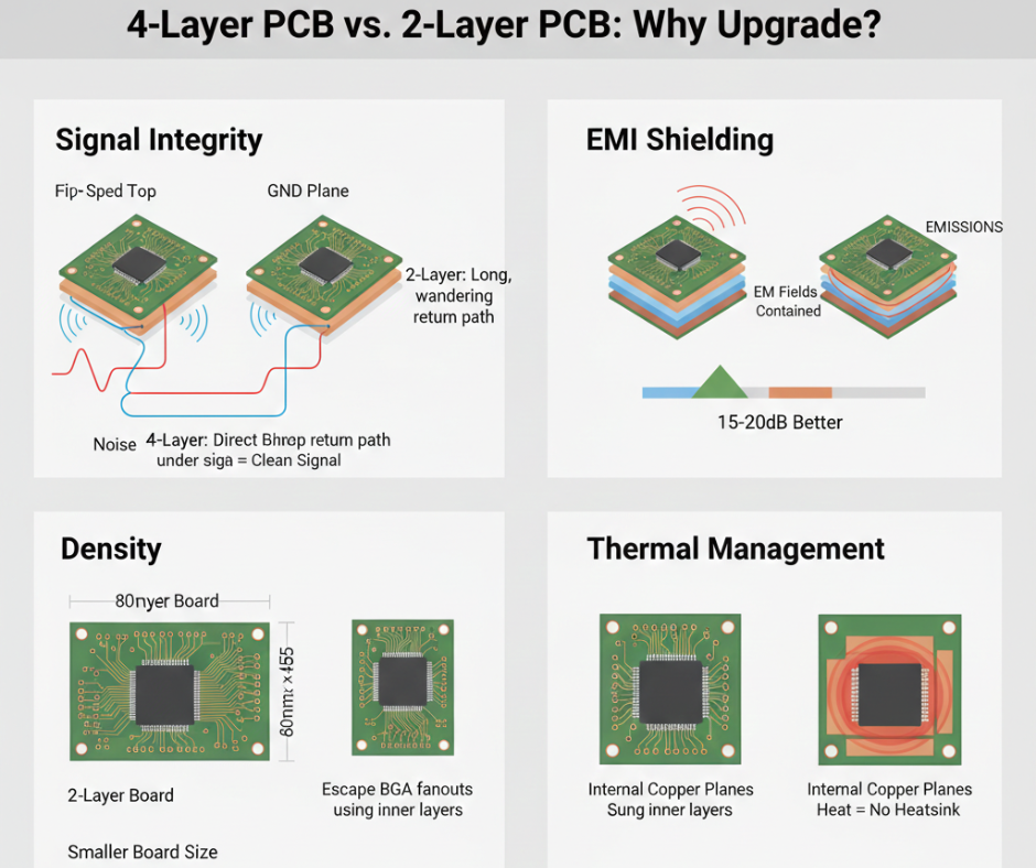
You design a 2-layer board. It works on the bench. Then you build 500 units, and they fail EMC testing. Sound familiar?
Signal Integrity
High-speed signals hate 2-layer boards. When you run a 100MHz SPI bus or USB 2.0 differential pair on a 2-layer design, the return current has to find its way back through whatever ground path you gave it. Usually, that means a long, wandering route through ground traces. This creates a big loop antenna that radiates noise and gets interference.
On a 4-layer board, return current flows directly under the signal trace through the ground plane. The loop area shrinks to almost nothing. Your signal eyes open up clean on the oscilloscope.
EMI Shielding
Those internal ground and power planes act like shields. They trap electromagnetic fields between layers instead of letting them radiate into space. You should test identical circuits on 2-layer versus 4-layer boards. The 4-layer version typically shows 15-20dB better radiated emissions. That is the difference between passing and failing FCC Part 15 Class B limits.
Density
You get four routing layers instead of two. Obviously, this lets you shrink board dimensions. But the real benefit is escaping dense components like BGAs or QFN packages with 0.5mm pitch. On a 2-layer board, you are limited to routing between pads. On a 4-layer board, you punch vias and drop to the inner layers to escape the rat’s nest.
A design that needs 80mm × 60mm in a 2-layer often fits in 60mm × 45mm with a 4-layer. That board area reduction can offset the higher per-board cost when you are building thousands.
Thermal Management
Copper conducts heat 200 times better than FR-4. Those internal planes spread heat across the board instead of letting it concentrate under your voltage regulator or MOSFET. For power supplies pushing 3A or more, this matters. You can sometimes eliminate a heatsink by using thermal vias to an internal copper plane. Saved me $1.50 BOM cost on a 12V PSU design by dumping heat into Layer 3 instead of bolting on aluminum.
The cost difference? Prototype quantities run $15-30 more per board for 4-layer versus 2-layer from most Chinese fabs. Production pricing at 1000+ pieces adds maybe $2-4 per board. Meanwhile, a single failed EMC test costs $3000-5000 for the retest alone. Do the math.
Key Design Specifications & Material Selection
FR-4 is your standard material. Period. About 95% of 4-layer boards use it because FR-4 costs one-tenth what specialty materials cost.
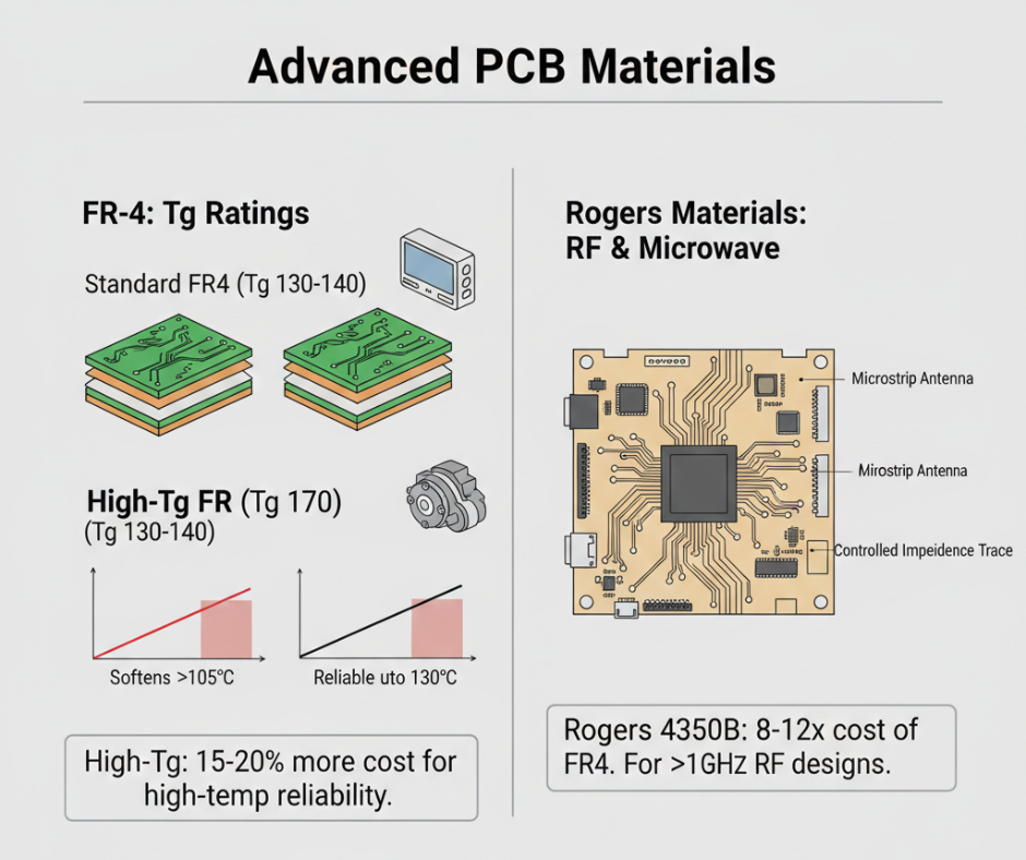
You will see FR-4 listed with different Tg ratings: TG130, TG150, TG170. This is the glass transition temperature where the material softens. Standard TG130-140 works fine for consumer products. You need TG170 for automotive or industrial gear that sits in hot enclosures or near engines. High Tg costs 15-20% more but gives you reliability at 130°C ambient instead of just 105°C.
Rogers materials enter the picture for RF designs above 1GHz. Rogers 4350B runs about 8-12 times the cost of FR-4. You use it when you need tight dielectric constant control for microstrip antennas or impedance-critical transmission lines.
Board Thickness
Standard is 1.6mm. This fits standard PCB slots in enclosures and provides good mechanical stiffness for hand assembly. You can order 0.8mm for ultra-thin devices like wearables, 1.0mm for cost-sensitive designs, or 2.0mm for high-current power boards. Just know that going thinner than 1.6mm makes the board flex more during assembly, which can crack solder joints on large components.
Copper Weight
Outer layers typically use 1oz of copper. This handles 3-4A per trace with reasonable trace widths. Inner power and ground planes usually spec 1oz as well, though some manufacturers default to 0.5oz on inner layers to save cost. Watch this on your quote.
For high-current designs pushing 10A+, you can order 2oz or even 3oz copper, but it costs more and limits your minimum trace width since thicker copper is harder to etch fine features.
Impedance Control
This is where 4-layer boards shine. You need controlled impedance for USB, Ethernet, HDMI, or DDR memory. The calculator spits out a trace width based on your stackup geometry. A typical 50Ω microstrip on a 4-layer board with 1oz copper and 10mil dielectric spacing runs about 12-15 mils wide. Manufacturers charge $50-150 extra for impedance control because they need to test coupons and certify the results.
You need to provide your fab house with a stackup specification if you want controlled impedance. Telling them I need 50 ohms without defining the dielectric thickness and Er value leaves them guessing. Many times they guess wrong.
Manufacturing Capabilities
Your design is only as good as what the fab can actually build. Here is what standard 4-layer capabilities look like at decent Chinese manufacturers as of 2026:
Minimum Trace
4mil/4mil is achievable at most shops without premium pricing. This lets you route between 0.5mm pitch BGA pads. You can push to 3mil/3mil or even 2.5mil/2.5mil, but expect upcharges and longer lead times. For most designs, 5mil/5mil or 6mil/6mil works fine and keeps costs down.
Minimum Hole Size
Mechanical drilling goes down to 0.2mm diameter. Anything smaller needs laser drilling, which triples your via cost. Standard vias run 0.3mm holes with 0.6mm pads. These are cheap and reliable.
Surface Finishes
HASL costs the least but leaves an uneven surface that causes problems for fine-pitch components below 0.5mm. ENIG adds $15-25 to prototype costs but gives you a flat, oxidation-resistant surface good for 12+ months’ shelf life.
You can use ENIG for anything with QFNs or BGAs. OSP sits in the middle of cost and shelf life, good for 6 months. Immersion Silver performs similarly to ENIG at a slightly lower cost but tarnishes faster.
Solder Mask Colors
Green is standard and free. Black looks professional, but makes inspection harder since you cannot see traces under the mask. White works great for LED boards because it reflects light. Blue and red are aesthetic choices that add $10-20 to prototypes. Matte black is trendy now for consumer products, but costs even more.
Blind and Buried Vias
Most 4-layer designs use standard through-hole vias that drill all the way through. Blind vias or buried vias let you route denser designs, but add significant cost. Expect 3-5× higher pricing. Avoid them unless you absolutely cannot escape a 0.4mm BGA otherwise.
Main Applications of 4-Layer PCBs
You find 4-layer boards everywhere in modern electronics.
Power Supplies
Switch-mode power supplies above 15W almost always use a 4-layer construction. The ground plane reduces switching noise, and the power plane distributes high currents without fat traces. We designed an 80W LED driver on a 2-layer board once. It worked, but radiated so much noise that it interfered with the AM radio in the customer’s facility.
Consumer Electronics
Smart home devices, WiFi routers, Bluetooth speakers, and anything with wireless connectivity need a 4-layer design to pass FCC testing. The antenna performance alone justifies the cost because ground plane placement directly affects radiation patterns and efficiency.
Automotive Controllers
Automotive electronics face harsh EMI environments with alternator noise, ignition spikes, and motor commutation interference. Four-layer boards with proper ground planes survive this electrical storm. Also, automotive temperature specs demand TG170 material that performs from -40°C to +125°C.
Industrial Control
PLCs, motor drives, and industrial HMIs use 4-layer boards for noise immunity. When you install equipment in a factory next to VFDs and welders, you need all the shielding you can get.
LED Drivers
High-power LED drivers benefit from the thermal spreading of internal copper planes. A 50W LED driver on a 4-layer can distribute heat through Layer 3, reducing hotspot temperatures by 15-20°C compared to a 2-layer.
How to Reduce Your 4-Layer PCB Price
Prototype pricing makes people nervous. You see quotes for $180 for five boards and wonder if production will bankrupt you. It will not.
Quantity
Five prototype boards from a Chinese fab run $100-200, depending on size and features. But 100 boards might cost $300-400 total. The setup cost gets amortized. By the time you hit 1000 pieces, you are looking at $3-6 per board for a standard 100mm × 100mm design. Do not make production decisions based on prototype quotes.
Via Technology
Through-hole vias cost almost nothing. Blind or buried vias multiply your cost by 3-5× because they require multiple lamination cycles. Unless you are designing a phone or ultra-compact wearable, stick with through-hole vias.
Board Size and Panelization
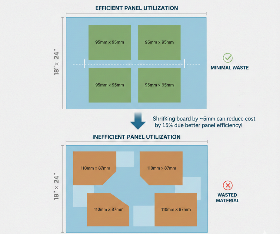
Manufacturers build PCBs on standard panel sizes, usually 18″ × 24″. If your board dimensions allow multiple copies per panel with minimal waste, the price drops. A 95mm × 95mm board fits four per panel with good utilization. A 110mm × 87mm board fits awkwardly and wastes material. Sometimes shrinking your board by 5mm cuts per-unit cost by 15% just from better panel efficiency.
Lead Time
Standard lead time runs 7-10 days from Chinese manufacturers. Rush service costs 2-3× more. Unless you are racing to a trade show, use standard lead time.
Design Complexity
Impedance control, fine pitch traces below 5mil, or heavy copper 2oz+ all trigger upcharges. Keep your design manufacturable with standard specs, and the quotes stay reasonable.
One more thing about cost: do not cheap out on surface finish to save $15 per board. A client saves $200 on 200 boards by using HASL instead of ENIG. Then they spent $4000 reworking 30% of the boards because the uneven surface caused tombstoning on 0402 resistors during reflow.
Summary
Four-layer PCBs cost more than 2-layer boards but deliver better signal integrity, EMI performance, and routing density. The standard stackup places ground and power planes internally with signal layers on top and bottom. This configuration handles high-speed signals, passes EMC testing, and allows denser component placement. Upload your Gerber files to get instant quotes and DFM feedback before committing to production.
About Wonderful PCB
Wonderful PCB handles everything from industrial design and electronic engineering to 4-layer PCB fabrication. We work with global companies to manufacture and assemble 4 layer printed circuit boards in China.
FAQ About 4-Layer Circuit Boards
Can I use a 4-layer board for high-frequency designs?
You can incorporate 6GHz with standard FR-4. Beyond that, you need Rogers or other low-loss materials. The important thing is controlling your dielectric constant and keeping your stackup symmetrical. For 2.4 GHz Wi-Fi, Bluetooth, or sub-1 GHz ISM-band designs, FR-4 works well. I have built GPS receivers on FR-4 without issues.
What is the standard thickness of the internal core?
For a 1.6mm finished board, the core is generally 1.0mm thick. The two prepreg layers add 0.3mm each. You lose about 0.07mm to copper thickness. It will give you roughly 10-12 mils of dielectric between Layer 1 and Layer 2, which is perfect for 50Ω controlled impedance traces.
How do I export Gerber files for a 4-layer PCB?
You need separate Gerber files for each layer, plus drill files. Export Top Copper, Ground Plane, Power Plane, Bottom Copper, Top Soldermask, Bottom Soldermask, Top Silkscreen, Bottom Silkscreen, and board outline. Add NC Drill files for through-holes. Most modern CAD tools, KiCad, Altium, and EAGLE, have 4-layer templates that export everything correctly. The manufacturer needs to know which inner layer is grounded and which is powered. Include a stackup drawing or note file specifying Layer 2 = GND and Layer 3 = VCC.