
PCB Manual Visual Inspection

Manual visual inspection of PCB boards is a very basic and simple type of inspection. For performing the manual inspection of the PCB board, engineers looked at the board with the use of any magnification process or checked the board with the naked eye.
In this inspection, the board made for final assembly is compared with the design requirements, either the manufactured board has all components connected at accurate points. The engineers identify various faults, which can be attributed to the type of board and the components connected to it.
The main benefit of manual visual inspection is we can get it if we perform at each phase of PCB manufacturing, also for assembly.
WonderFulPCB performs a manual visual inspection of each board with the use of magnifications, and we as professionals and skilled manufacturers follow the latest techniques for this inspection of the board.
Our inspection teams check almost every point and factor of the board to find any minor faults on the board.
Main checking point for visual inspection
- We check in visual inspection that board thickness is accurate according to design requirements and also make sure that proper roughness for the board surface.
- The final board assembly has the same dimensions as needed, and also check the dimensions related to connectors.
- There is a conductive pattern quality check with open circuits, short circuits, voids, and any solder bridging found.
- This test also detects dents, pinholes, pits, traces, and pad faults.
- The accurate position for vias is to make sure through this test and confirm that they are not punched at the wrong point and their diameter is according to design.
- Some other factors checked in this inspection are
- Components Missing
- misaligned components
- Component value added is not according to requirements.
- Broken components
- Open lead
- Polarity of components not accurate
Manual Visual Inspection Advantages
- It is a low-cost process, and there is no need for any special types of instruments for board inspection.
- It is a fast process, and we can use it at the end of any step of manufacturing.
- Make sure that the worker who is performing this inspection knows which point is needed to assess.
Automated Optical Inspection (AOI)
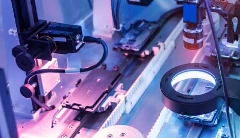
For performing visual inspection of PCB boards, an inspection machine is used, and this process is known as automated optical inspection (AOI).
The AOI techniques come with a computer, PCB board reader, light sources, and camera. In this process, with the use of a camera PCB board, photos from different points were taken and then compared with an original design to find any faults and errors.
The AOI inspection process is a faster process as compared to manual visual inspection since it is performed with the use of certain instruments and has less chance of human error.
AOI inspection is performed in 2D and 3D types, but it makes automated inspection of the board costly.
The other replacement for this process is the use of light sources that operate with lasers. This laser power-based system checks the PCB board through the use of reflected beam intensity. With the use of these instruments, we can find board solder deposition, clarity, alignment, etc.
It is a beneficial process to use a laser-based system, but it is a time-consuming process since, before using this device, we needed to calibrate each board for inspection with instruments to avoid shielding.
The main errors found in AOI inspections are
- It found the polarity of components
- Solder fillet
- Upside down
- Markings
- Billboards
- Missing Lead
- Component dimensions
- Coplanarity
- Short circuits
- Line width violations
- Bridging
X-ray Inspection
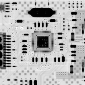
With advancements in SMT techniques, PCB boards are becoming complicated to design. Currently, most of the boards are densely structured and have small-sized component connections that come with chip packages, BGA, and chip scale packages that make it difficult to check the solder connections. For the detection of hidden or difficult-to-access solder connections, the use of manual and automated inspection techniques is not a good option.
To solve these issues, an inspection of such complex designs uses X-ray inspection techniques.
How X-ray Inspection Works?
To understand the X-ray inspection, you must know that each material has different capabilities to absorb the X-ray based on its atomic weight value. Heavyweight components absorb more rays than lighter weight, and it will help to differentiate faulty components.
Silver lead and tin are heavy elements that are used for the creation of solder, and connected components on boards are made with less-weight components such as copper, carbon, etc. So solder that is dense can easily be seen with the use of X-ray inspection, and different components like leads and ICs are not easy to see.
In X-ray inspection, rays are not reflected but pass through components and make an image of the object. In this way, we can easily observe chip packages and connected components to check the connections of connected components beneath.
With the use of X-ray inspection, we can also see solder joint bubbles that are not easy to see with an automated inspection.
For dense board X-ray inspection, it is the best option since it also helps to see solder joints that are not seen with AOI.
There are manual X-ray inspections and automated X-ray inspections (AXI) that can be performed for the board based on requirements.
For through-chip packages and complicated boards, X-ray is the best option where other methods do not work well. It is the best technique for complex design, but it is now costly since the new technique.
For your PCB board that needs professional and the latest inspection techniques, WonderfulPCB offers quality X-ray services with advanced instruments. We will provide your quality services in a professional way and the use of advanced instruments.
Flying Probe Testing
Flying probe testing is a circuit testing technique that uses probes for making electrical connections with testing points of PCB assembly testing. In this process, we flow probes on the board surface and make connections to the points, finding results that match already set points. This testing method is used for high-volume production.

How Does the Flying Probe Test Work?
For testing some circuits, flying probe testing is the best to use since it is a fast and low-cost option. This test is also used for testing prototypes before making the final assembly. The process for this test is explained here.
- First of all, make a test program for performing flying probe tests. That program will have detailed instructions for probes for board testing, like test type, voltage level employed, and point where testing is performed on board.
- After finalizing the program, move the test probe on board. The features of probes are such that they can move in any direction on board for testing.
- When the probe is at an accurate point where our instructed program is applied. The probe makes contact with testing points on board and uses a set voltage level. Our program will measure different electrical factors such as the value of current resistance, inductance, and capacitance.
- After completion of the test, results are checked to find whether the board is working according to requirements or not. If there is any error on board, that will be solved by our engineers.
The main purpose of using a flying probe test is to find different factors, such as on the PCB board.
- Capacitance
- Diode Inspection
- Inductance
- Opens
- Resistance
- Short Circuits
FPT is a very important technique for PCB manufacturing testing and also for PCBA testing and provides high-performance and reliable electronic projects.
In-Circuit Testing (ICT)

In-circuit testing, or ICT testing, is a testing method performed for testing different components connected to a PCB board and their connection with the board. This test helps to find out if they are accurately connected on board.
This test is performed at the start of production, which helps to find and solve any error on board to avoid faulty final electronic products.
In this test, the board is connected with testing devices that have probes and probes connected to the board and find different factors such as inductance, resistance, short circuit, and capacitance that make sure components connected to boards are at accurate points.
Through this process, we can find manufacturing faults and assembly errors and make the final assembly for the board accurately working.
For performing the ICT test, the IC tester comes with different probes that have features to test many points on the board, and these probes can be programmed for different testing features.
Functional Testing (FCT)
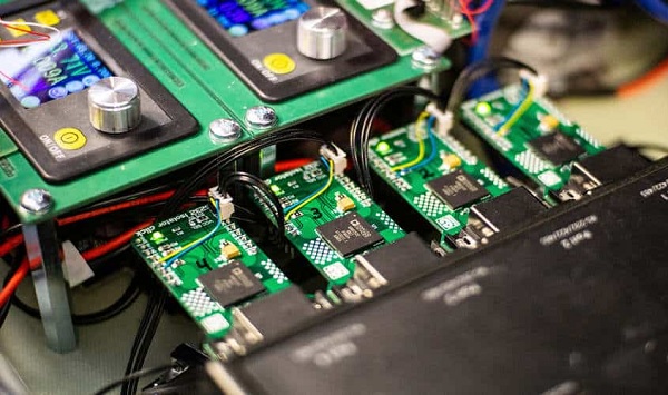
This test performs as the last point of inspection and final assembly verification. The main purpose of this test is to check board functions and integrity. This test is normally performed after the assembly process or during board manufacturing. The other name for the functional test is the function verification test.
Through performing this, we make sure that all connected components on boards are working well and according to design requirements.
The main function of this test is to stimulate board input and output signal values such as current, volts, and power by getting a response from components.
For performing this test, a dedicated FCT testbed was used to make sure that the board was working well. High current during the test helps to find errors and give details for the board’s proper working. The FCT test also helps to find errors that were not found at the time of visual inspection.
Burn-In Testing

Burn-in testing employs high stress on board for finding errors and developing load capacity. The high-pressure applications on board give board strength and load-handling features before use in practical projects. This test is normally performed to check that the board is reliable for any final electronic device assembly.
- There are two types of burn-in in the test: the first one is static burn-in in the test, and the second is dynamic testing.
- Static burn-in is a test performed where the PCB is not in working mode when high voltage and temperature are applied. While for dynamic tests, the PCB board is in operational mode when high temperature and voltage are applied. A dynamic test is performed for a complex design board.
Solderability Testing

This test is used for finding solderability features of leads and terminals that are performed through the use of different soldering processes.
Solderability is the parameter that measures the perfection of metal wet through molted solder for making connections.
By conducting the solderability test for the PCB board, we can determine that connected components like leads and terminals have features to handle high-temperature conditions. High temperature is the result of the welding process; through tests, we can also find that component storage will badly affect their features for board soldering.
Solderability is a molten solder feature to maintain smooth liquid conditions unaffected at the time of the soldering process.
Fixture testing
The PCB test fixture called a test jig or test rack, is a certain type of tool that is used for checking the PCB board’s functionality and working performance at the time of the manufacturing process. In this testing technique, nodes, connected components on the board, and signals flowing on the board are tested.
The PCB test fixture is a special type of tool that holes and connects with the board at the time of testing. It provides an electrical connection between UUt and external testing devices.
It helps to signal flow to UUT and as a result, value measured and handle UUT in and out of the fixture.
The PCB test fixture comes with test points put on the board and test probes that make connections with testing points. The fixture operates manually or automatically according to design requirements and production volume.
This test helps to find defects at the start, and we can correct them timely and help to make fast development of electronic products in a short time.
These testing techniques provide repeated testing features that help us to make fully working and reliable boards.
PCB Testing at WonderFulPCB
WonderfulPCB is the best supplier of PCB services, and we also perform different PCB testing processes. The main objective is to provide high-quality and error-free PCB and PCBA-based services for our customers. For quality board manufacturing PCB testing is the main part and before starting production our engineers deeply check the Gerber files to make sure that the design is correct and if there is any error exists can be solved at the start
At WonderFulPCB, different PCB tests and PCB testing processes are performed such as visual inspection, Automated Optical Inspection (AOI), and Flying Probe Testing. We maintain quality and reliability in our products for our customers.
We have been working in the PCB industry since 1995, and our main focus is to provide quality services for our clients. So each of our products and boards goes through a detailed testing process to fulfill the requirements of our customers for optimal performance and functions that are part of our PCB fabrication process.