The most dangerous thing about a 6 layer PCB is not the design complexity. It is the assumption that a fab’s ‘standard’ stackup is safe. That assumption cost one real project $13,000, 18 days of schedule slip, and a delayed customer demo — all because two inner signal layers were adjacent without a plane between them.
Every guide on 6-layer PCB design will tell you to add layers when your 4-layer board gets too crowded. That advice has launched a thousand failed responses. Layer count is an electrical architecture decision with signal integrity, yield, and total-cost consequences that compound in ways most first-time 6-layer designers do not see until they are staring at a failed bring-up.
What Is a 6 Layer PCB Board?
Definition and Basic Structure
A 6 layer PCB is a printed circuit board built from six conductive copper layers laminated together with insulating dielectric material. The copper layers carry signals, distribute power, and provide electromagnetic reference planes. The dielectric layers — typically prepreg and solid core material — separate and insulate the copper layers from each other. All six layers are electrically connected through drilled and plated holes called vias.
Unlike a 2-layer board where all routing and all power distribution must share the two outer surfaces, a 6-layer board allows signals to be routed on inner layers shielded by reference planes, power and ground to occupy dedicated inner layers, and outer layers to be reserved for component connections and accessible signals.
How a 6 Layer PCB Differs from 2-Layer and 4-Layer Boards
| Feature | 2-Layer | 4-Layer | 6-Layer |
| Routing layers | 2 | 2–3 | 3–4 |
| Dedicated ground plane | No | 1 typical | 1–2 typical |
| Dedicated power plane | No | 1 typical | 1 typical |
| EMI shielding of inner signals | None | Partial | Full |
| Impedance control ease | Difficult | Moderate | Good |
| Mixed signal isolation | Minimal | Split planes only | Separate plane pairs possible |
| Cost multiplier vs 2-layer | 1x | ~1.4–1.7x | ~1.8–2.2x quoted; 2.8–3.5x landed |
Key Components of a 6 Layer PCB
The physical build consists of three core substrates sandwiched with two layers of prepreg, all pressed under heat and pressure. The outer layers receive copper foil lamination. Copper traces are etched into each layer using photolithographic processes. A solder mask is applied to both outer faces to protect traces and define solderable pads. Surface finish is applied to exposed copper to prevent oxidation and enable soldering.
6 Layer PCB Stackup Explained
What Is a PCB Stackup?
The stackup is the ordered arrangement of copper and dielectric layers that defines the electrical and mechanical properties of the board. It determines impedance, capacitance between planes, signal isolation, EMI shielding effectiveness, and mechanical flatness. Getting the stackup wrong is the single most common cause of 6-layer bring-up failures — because it cannot be fixed without a complete respin.
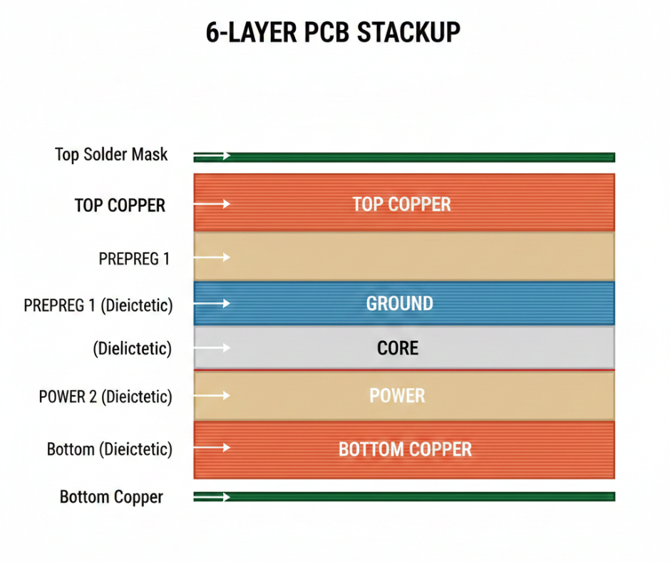
Standard 6 Layer PCB Stackup Configuration
The correct reference stackup for a general-purpose 6 layer PCB board with high-speed signals is a symmetric 3-core build:
| Layer | Function | Reference / Notes |
| L1 — Top Signal | Component side routing, fine-pitch BGA escape | Referenced to L2 GND — microstrip |
| L2 — Ground Plane | Solid GND — primary EMI shield | References L1 above and L3 below |
| L3 — Inner Signal | High-speed differential pairs, controlled impedance | Referenced to L2 above, L4 below — stripline |
| L4 — Power Plane | Primary power distribution VCC, VDDIO, etc. | References L3 above and L5 below |
| L5 — Inner Signal | Secondary routing, low-speed or isolated signals | Referenced to L4 above, L6 below — stripline |
| L6 — Ground / Bottom Signal | Bottom routing or solid GND return | Referenced to L5 above — microstrip |
Types of 6 Layer PCB Stackup Configurations
Not all 6 layer PCB boards use the same layer assignments. The configuration should be driven by the dominant design constraint:
• Standard SIG/GND/SIG/PWR/SIG/GND: Best general-purpose choice. All signal layers have adjacent plane references. Suitable for most mixed digital designs.
• High-Speed Stripline: Route all critical differential pairs on L3 and L5 , keeping L1 and L6 for lower-speed connections. Maximizes EMI shielding for >5 Gbps interfaces.
• Mixed-Signal: Assign L3 to analog signals with a dedicated analog GND on L2 and analog power split on L4. Digital domain occupies L5 and L6. Prevents digital switching noise coupling into analog front-end.
• Power Integrity Focus: Two separate power planes with a thick central core between them. Maximizes interplane capacitance for high-current switching regulators.
The Stackup That Will Ruin Your Bring-Up
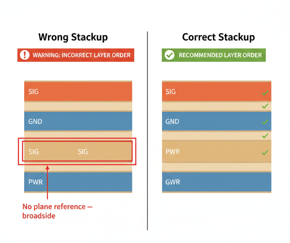
The most common failure pattern in first-time 6-layer designs: SIG / GND / SIG / SIG / PWR / GND. This places L3 and L4 as two signal layers directly adjacent with only thin prepreg between them and no plane reference for either. Return currents at via transitions have nowhere to go. Broadside crosstalk between L3 and L4 is uncontrolled. A real 2022 PCIe Gen2 project using this exact stackup produced differential impedance variation of 92–108 ohms instead of the 85-ohm target — causing lane failures on 50 assembled boards.
Best vs. Worst 6-Layer Stackup Configurations
A 6-layer board with a bad stackup — particularly two adjacent signal layers in the middle — radiates more EMI than a well-executed 4-layer board with a solid GND on L2. The plane layer provides the primary EMI shielding mechanism. Every signal layer must be adjacent to a plane on at least one side; burial between two planes is better. The worst configuration is any arrangement that leaves a signal layer without a nearby plane reference.
Dielectric Materials Used in 6 Layer PCB Stackups
| Material | Dk | Loss Tangent | Best For |
| FR-4 | 4.2–4.5 | 0.018–0.025 | General digital, <5 Gbps |
| Rogers RO4350B | 3.48 | 0.0037 | RF, >10 GHz, controlled Dk |
| Isola FR408HR | 3.65 | 0.009 | High-speed digital, 5–25 Gbps |
| Panasonic Megatron 6 | 3.4 | 0.004 | Backplane, >25 Gbps SerDes |
6 Layer PCB Thickness and Dimensions
Standard 6 Layer PCB Thickness Options
Standard finished thickness options for 6-layer boards are 1.0 mm, 1.2 mm, 1.6 mm, and 2.0 mm. Each thickness requires a specific combination of core and prepreg thicknesses to hit the finished dimension, which directly affects the dielectric spacing between layers and therefore the achievable impedance values.
Why 1.6mm Is the Most Common Thickness
The 1.6 mm build is dominant in 6-layer designs because it accommodates standard core-and-prepreg combinations that produce a symmetric stackup without special material orders. It is the default offering at nearly every commercial fab, meaning lead times are shortest and pricing is most competitive. For most digital and mixed-signal designs with no aggressive enclosure constraints, 1.6 mm is the right starting point.
How to Choose the Right PCB Thickness
Thinner builds require thinner dielectric layers, which reduce the spacing between adjacent planes and signal layers. This increases interplane capacitance but makes impedance control harder without a custom stackup. A real project example: specifying controlled impedance on a 1.2 mm board forced a change to 1.6 mm because the required dielectric thicknesses for 85-ohm differential pairs did not fit within the thinner build — violating the mechanical enclosure clearance. Always confirm enclosure constraints before locking in the stackup.
Copper Weight and Trace Width Specifications
Most 6-layer boards use 1 oz copper on outer layers and 0.5 oz copper on inner layers as the default. Heavier copper is available for high-current applications but requires wider trace spacing and minimum via annular ring adjustments. Minimum trace width on standard 6-layer processes is typically 3–4 mil outer, 3.5–4 mil inner; minimum spacing mirrors these values. BGA escape routing commonly requires 3/3 mil trace-space at 0.8 mm pitch.
6 Layer PCB vs 4 Layer PCB: When to Upgrade
The Most Dangerous Misconception
The most common reason to go to 6 layers: routing got tight on the 4-layer board. Layer count is not a scalability dial. A crowded 4-layer board with good SI is better than a 6-layer board with a broken stackup. Adding layers to escape a routing problem often just moves the problem deeper into the board where it is harder to debug.
The Real Triggers for Moving to 6 Layers
The decision to go to 6 layers should be driven by specific, identifiable electrical constraints that cannot be solved on 4 layers:
• You have exhausted reference plane adjacency for critical signals — every high-speed signal needs a return plane on the immediately adjacent layer, and your 4-layer stack cannot provide it.
• You simultaneously need multiple independent return paths: digital, analog, and RF domains that would couple destructively if sharing a single plane pair.
• You are routing more than 8 to 10 high-speed differential pairs above 500 MHz edge rate from a BGA where the escape consumes both outer layers, leaving no reference for inner signals.
• You need dedicated power plane spreading inductance that split planes on a 4-layer board cannot achieve.
When a 4 Layer PCB Is Still Sufficient
A dense board with signals below 50 MHz can remain on 4 layers indefinitely with disciplined fanout, orthogonal routing, and via optimization. Many IoT and low-speed industrial control boards are over-specified into 6 layers when a routing review and component placement optimization would solve the 4-layer constraint cleanly.
Cost Comparison: 4 Layer vs 6 Layer PCB
The quoted price for a 6-layer board is typically 1.8 to 2.2 times the equivalent 4-layer board at the same size and copper weight. This is the number that appears in RFQs. The real landed cost multiplier — after accounting for prototype respins, yield-adjusted scrap in volume, and NRE for cross-section verification — runs 2.8 to 3.5 times the 4-layer equivalent. One 2023 production project quoted at $18 per unit at 500 pieces landed at an effective $62 per unit after two resins and yield losses. Budget for the real multiplier, not the quoted one.
6 Layer PCB Design Guidelines
Signal Routing Best Practices
Route high-speed differential pairs on inner signal layers where they are buried between two plane layers. Inner stripline routing provides better EMI shielding and more predictable impedance than outer microstrip. Avoid routing critical signals on outer layers unless the design has no inner layer routing option — outer signals radiate more readily and are more susceptible to assembly-related damage.
Use orthogonal routing directions between adjacent signal layers. If L1 routes predominantly in the X direction, L3 should route predominantly in the Y direction. This minimizes via-to-via crosstalk at layer transitions and makes impedance-controlled routing easier to achieve with consistent trace geometries.
Power and Ground Plane Design
A 6-layer board’s power integrity advantage comes from the tight coupling between the PWR and GND plane pair. Maximize this by keeping the dielectric between L4 and the adjacent GND as thin as manufacturing allows — 4 to 6 mil prepreg in a standard build. Place decoupling capacitors within 200 mil of each IC power pin, with the via to the power plane and the via to the ground plane placed symmetrically on either side of the capacitor body. Avoid routing signal traces through splits in the power plane — return current must cross the split, creating a loop that radiates.
Impedance Control in 6 Layer PCBs
Controlled impedance in a 6-layer board depends on the dielectric thickness between the signal layer and its nearest reference plane, the trace width, and the dielectric constant of the material. Inner stripline layers achieve tighter impedance tolerance than outer microstrip layers because they are shielded from surface effects and lamination variation is more consistent in the center of the build.
Expert nuance: a 0.5 mil variation in prepreg thickness — well within a typical fab’s process window — shifts a nominally 50-ohm stripline trace to 58 ohms. At 8 Gbps, this closes the eye. Always verify impedance test coupon data on the first article build, not just the stackup specification.
Controlled impedance is not always the right specification. A 2024 medical device design carried USB 3.2 Gen1 at 5 Gbps on traces under 40 mm with only two layer transitions. Specifying controlled impedance would have added 38% to the fab cost, extended lead time by 3 weeks, and forced a thicker board that violated the enclosure. The board was built on a standard stackup with 7/7 mil trace-space, series damping resistors, and length matching to 5 mm. It passed EMC and functional validation on the first spin. Controlled impedance callout is essential for >10 Gbps, traces over 150 mm, and multi-transition BGA routes — not for every differential pair.
Via Types Used in 6 Layer PCBs
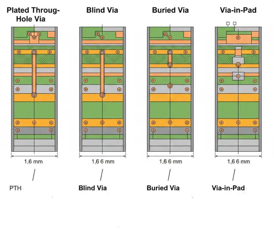
• Plated Through-Hole: Standard via connecting all six layers. Low cost, universally available. Via stub below the last used layer creates resonance above 3 GHz — use back-drilling if this matters.
• Blind Vias: Connect outer layer to inner layer only. Eliminate via stub. Required for fine-pitch BGA escape on dense boards. Add 25–40% to fab cost.
• Buried Vias: Connect inner layers only, invisible from the board surface. Used in extreme density HDI designs. Significant cost adder; require sequential lamination.
• Via-in-Pad: Via drilled directly through the SMD pad. Allows tightest BGA pitch. Must be filled and capped to prevent solder wicking during reflow. Standard for 0.5 mm pitch BGA.
EMI and EMC Design Considerations
The primary EMI mechanism in a digital 6-layer board is the loop formed between a signal trace and its return current path on the adjacent plane. Minimize this loop by never routing a signal trace across a plane split or over a gap in the reference plane. Use via stitching — ground vias placed at regular intervals around the board perimeter and between signal regions — to create low-impedance return paths at layer transitions. Place stitching vias within 200 mil of every signal via on a high-speed net.
Thermal Management in 6 Layer PCB Design
Place thermal vias in a grid pattern under exposed pad components connecting the top-side pad directly to inner GND planes. A grid of 0.3 mm diameter vias at 0.6 mm pitch provides effective thermal spreading into the inner copper mass. For high-power sections, the inner PWR and GND planes act as heat spreaders that distribute thermal load before it reaches the PCB edge or an external heat sink.
6 Layer PCB Manufacturing Process

Step-by-Step: How a 6 Layer PCB Is Made
• Step 1 — Inner core preparation: The two inner core substrates are coated with copper foil, exposed with the circuit pattern photolithographically, and etched to leave only the designed copper traces and planes.
• Step 2 — Oxide treatment: Inner copper surfaces are chemically treated to improve adhesion between copper and prepreg during lamination.
• Step 3 — Lamination: All layers — cores, prepreg sheets, and outer copper foils — are stacked in precise alignment and pressed under heat and pressure until the prepreg resin flows and cures.
• Step 4 — Drilling: Mechanical drilling creates through-holes for PTH vias and component holes. Laser drilling creates blind micro-vias for HDI designs. Via location accuracy at this step determines the layer-to-layer registration quality.
• Step 5 — Copper plating: The drilled holes are plated with electroless copper followed by electrolytic copper to build up via wall thickness.
• Step 6 — Outer layer etching: Outer copper foil is patterned and etched to create L1 and L6 traces, pads, and planes.
• Step 7 — Solder mask application: Liquid photo-imageable solder mask is applied, exposed, and developed to cover traces while leaving pads exposed.
• Step 8 — Surface finish: Final surface finish is applied to exposed copper pads.
• Step 9 — Testing and inspection: Electrical continuity and isolation testing, AOI, cross-section analysis, impedance verification on test coupons.
The Registration Tolerance Problem — Why It Matters More Than the Spec Sheet
Mid-tier fabs typically hold layer-to-layer registration at ±0.075–0.1 mm on 6-layer builds, compared to ±0.05 mm on 4-layer. At 0.15 mm via size, this registration tolerance can move the via annular ring to the edge of minimum IPC Class 2 compliance. Boards that pass flying-probe electrical tests can still have structurally weak vias that fail under thermal cycling stress in the field. This is the hidden yield problem that does not appear until volume production.
Surface Finish Options
| Surface Finish | Best Application | Key Consideration |
| ENIG | Fine-pitch BGA, wire bonding | Black pad risk if Ni/Au thickness not controlled |
| HASL Lead-Free | Cost-sensitive, through-hole dominant | Uneven surface on <0.5mm pitch SMD |
| OSP | High-volume SMD, single reflow | Shelf life <12 months; poor for rework |
| Immersion Silver | High-frequency RF, >10 GHz applications | Tarnish-sensitive; requires careful storage |
| Immersion Tin | Press-fit connector applications | Tin whisker risk if not properly specified |
Quality Testing and Inspection
Automated Optical Inspection scans all six layers post-etch and post-assembly for opens, shorts, and missing features. Electrical flying-probe or bed-of-nails testing verifies continuity and isolation on every net. For controlled impedance designs, test coupons placed on the panel perimeter are cross-sectioned and measured with a TDR to verify the as-built impedance against the specification. Cross-section analysis is performed on sample boards from each lot to measure dielectric thickness, copper plating uniformity, and via registration accuracy.
6 Layer PCB Cost Factors
What Determines the Price of a 6 Layer PCB?
The quoted unit price is driven by board dimensions, copper weight, material selection, via complexity, surface finish, and order quantity. Each of these variables is visible in the RFQ. The variables that are not visible — and that dominate total project cost — are yield, respin probability, and process verification NRE.
| Cost Driver | Quoted Price Impact | Hidden / Landed Cost Impact |
| Board size | Direct — price per panel area | Low — predictable |
| Material | 2–5x increase for specialty | Moderate — specialty lead times can extend |
| Via type | +25–40% for blind vias | Moderate — offset by density savings |
| Surface finish | +$0.50–2.00/unit for ENIG | Low — predictable |
| Order quantity | Standard volume discount | Low — predictable |
| Layer registration tolerance | Not visible in RFQ | HIGH — drives yield loss at volume |
| Dielectric thickness variation | Not visible in RFQ | HIGH — drives SI respins |
| Impedance coupon NRE | Sometimes quoted, often not | HIGH — added silently on 2nd–3rd order |
| Cross-section verification | Sometimes quoted, often not | HIGH — required after any yield event |
The Real Cost Multiplier — What Procurement Needs to Know
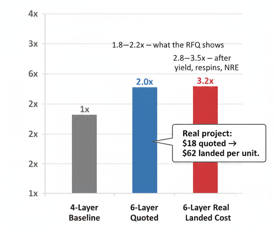
The real-world ratio from production tracking: a 6-layer board quoted at 1.8 to 2.2 times the 4-layer equivalent lands at 2.8 to 3.5 times when yield loss, respin NRE, and process verification costs are included. First-pass yield at mid-tier Asian fabs on standard 6-layer builds runs 70 to 85 percent, versus 95 percent or higher for 4-layer. The scrap rate difference alone adds 10 to 25 percent to effective unit cost in volume.
How to Reduce 6 Layer PCB Costs Without Compromising Quality
• Standardize your stackup: Use the fab’s standard 6-layer build wherever your signal requirements permit. Custom stackups add setup cost and extend lead time.
• Match via size to the fab’s sweet spot: Designing via diameters at 0.2 mm or above avoids the tight-tolerance drilling that drives yield loss and cost.
• Reserve controlled impedance callout: Apply it only to the layers and nets that genuinely require it. Calling out controlled impedance on every layer adds fab cost and lead time without benefit on low-speed nets.
• Run a pre-production validation lot: 50 to 100 boards at full panel size before volume commitment. The cost of a validation run is always lower than the cost of a 20 to 30 percent scrap rate on the first volume order.
Applications of 6 Layer PCB Boards
The 6-layer cost premium is justified when the electrical requirements genuinely cannot be met on fewer layers. The applications where this is true share a common profile: multiple high-speed serial interfaces, mixed-signal domains requiring physical separation, or component densities that make 4-layer routing impossible without via compromises that break signal integrity.
• High-speed computing and server hardware: PCIe Gen3/4, DDR4/5, 25G Ethernet interfaces where impedance control and plane continuity at every via transition are mandatory, not optional.
• Communication equipment: Multi-port routers, switches, and base station modules where high-speed serial links coexist with analog power management and RF front-ends on a single board.
• Medical diagnostic devices: Analog front-end circuits requiring isolation from digital processing domains, with dedicated plane pairs for each signal domain to prevent switching noise coupling.
• Automotive ADAS and infotainment: High-speed video interfaces, CAN/LIN, and RF coexisting on a single board with strict EMC requirements and wide temperature range.
• Industrial control systems: Mixed-voltage designs with isolated analog measurement channels, high-current PWM outputs, and communication interfaces on a single board.
• Aerospace and defense: Applications where the cost premium is a secondary consideration compared to signal integrity, thermal reliability, and long service life requirements.
A 6-layer PCB is not simply a 4-layer board with more routing room. It is a fundamentally different electrical architecture with specific constraints on stackup, return current management, impedance control, and manufacturing process quality. The decisions made before a single trace is routed — stackup configuration, dielectric material, via strategy, vendor selection — determine whether the design succeeds on the first spin or becomes an expensive lesson.
The real cost of a 6-layer board is not the per-unit price on the RFQ. It is the sum of the quoted price, the expected respin cost, the yield-adjusted scrap rate in volume, and the process verification NRE that does not appear until the second order. Budget for 2.8 to 3.5 times the 4-layer equivalent as the planning number, and validate vendor process capability with real data before committing to volume.
Is a 6 Layer PCB Right for Your Project?
| Signal requirement | Stackup constraint | Recommendation |
| <50 MHz, moderate density | No high-speed reference plane requirement | Stay on 4 layers, optimize layout first |
| 500 MHz–5 Gbps, BGA, mixed signal | Need independent plane pairs per domain | 6 layers — use symmetric 3-core build |
| >5 Gbps SerDes, backplane | Tight impedance control, low-loss material | 6 layers minimum — consider specialty dielectric |
| RF + digital coexistence | Isolated GND domains required | 6 layers — dedicated analog/RF plane pair |
Quick Reference: Key Numbers
| Metric | Value |
| Quoted price multiplier vs. 4-layer | 1.8x–2.2x |
| Real landed cost multiplier | 2.8x–3.5x |
| First-pass yield — 6-layer, mid-tier fab | 70–85% |
| First-pass yield — 4-layer, mid-tier fab | 95%+ |
| Layer registration tolerance — standard 6-layer | ±0.075–0.1 mm |
| Dielectric thickness variation — typical | ±0.8 mil |
| Typical min. trace/space — standard 6-layer process | 3–4 mil / 3–4 mil |
| PCIe Gen2 respin (real project, 2022) | $13,000 + 18-day slip |
| Medical device: controlled impedance vs standard cost | $11.40 vs $8.25/board + 3-week delay |
| High-speed pairs threshold for considering 6 layers | >8–10 differential pairs >500 MHz edge rate |
Frequently Asked Questions About 6 Layer PCB Boards
What is the standard thickness of a 6 layer PCB?
The most common finished thickness is 1.6 mm, used by the majority of commercial fabs as their default 6-layer build. 1.0 mm and 1.2 mm are available for space-constrained applications but require custom stackup review. 2.0 mm is used in backplane and high-power applications. Confirm your enclosure constraints before specifying thickness — controlled impedance callout can force a thicker board than the default.
What stackup configuration is best for high-speed signals?
The symmetric 3-core build with the configuration SIG / GND / SIG / PWR / SIG / GND gives every signal layer a direct plane reference. Route the most critical high-speed differential pairs on L3 for best EMI shielding and most predictable impedance. Avoid any stackup that places two signal layers directly adjacent to each other without a plane between them.
How much does a 6 layer PCB cost?
Quoted unit price is typically 1.8 to 2.2 times the equivalent 4-layer board. Real landed cost — including prototype respins, yield-adjusted scrap in volume, and process verification NRE — runs 2.8 to 3.5 times the 4-layer equivalent. A project that was quoted at $18 per unit landed at an effective $62 per unit after yield events and two resins. Budget for the landed multiplier, not the quoted price.
When does controlled impedance become necessary on a 6 layer board?
Controlled impedance is necessary for signals above approximately 1 Gbps with trace lengths over 100 to 150 mm, or for any multi-gigabit interface with BGA escape routing involving multiple layer transitions. It is not always necessary for short traces at moderate speeds — a USB 3.2 Gen1 design with traces under 40 mm can be validated with TDR measurement on first-article boards and may pass without a formal impedance callout, saving fab cost and lead time.
What is the most important question to ask a PCB vendor before ordering a 6 layer board?
Ask for their actual layer-to-layer registration tolerance and dielectric thickness tolerance on a standard 6-layer build, supported by cross-section data from a recent similar panel. A vendor who answers with IPC class references instead of real numbers is a vendor whose process control you should not trust without an independent validation run.
Can I convert my 4 layer design to 6 layers?
Yes, but the conversion should not be mechanical. Simply adding two layers to an existing 4-layer layout without reconsidering the stackup architecture, reference plane assignment, and power distribution will not solve your signal integrity problems and may create new ones. Treat the move to 6 layers as a re-architecture exercise, not a board resize.
What software is best for 6 layer PCB design?
Altium Designer, Cadence Allegro, and KiCad 7+ all support 6-layer design with controlled impedance design rules and interactive high-speed routing. For 6-layer designs with SI requirements, the stackup editor and impedance calculator in the layout tool must be configured with the fab’s actual stackup data — not default values — before any impedance-critical trace is routed.