Overseas 8 layer PCB manufacturers have industrialized the appearance of quality. IPC certifications, ISO plaques, polished capability decks — these signals look reassuring and routinely obscure what actually happens on the shop floor. This guide gives you the procurement framework to evaluate overseas fabs based on process evidence, not sales materials.
What Is an 8-Layer PCB?
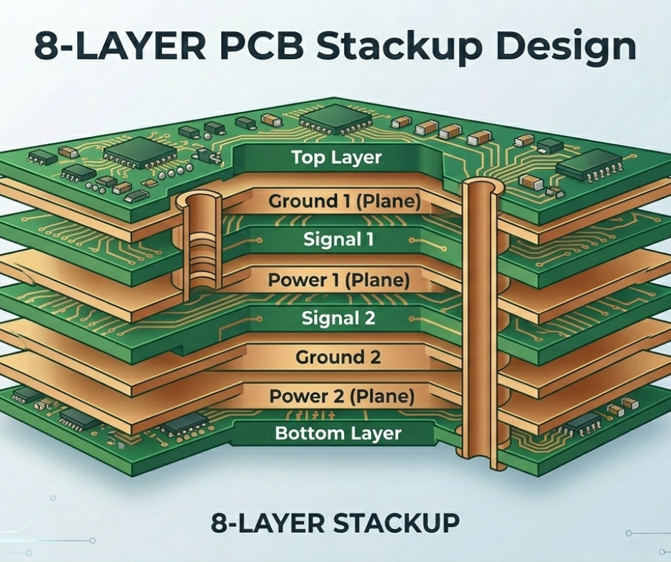
An 8-layer PCB is a multilayer printed circuit board with eight conductive copper layers separated by dielectric materials — alternating prepreg and core laminates — laminated under heat and pressure into a single rigid structure.
The standard layer arrangement assigns each layer a function:
- L1 and L8 are outer signal layers routed as microstrip traces
- L2 and L7 are ground planes
- L3 and L6 carry high-speed signals as striplines, fully enclosed between reference planes for controlled impedance
- L4 and L5 are dedicated power planes, tightly coupled to reduce power rail noise and support stable voltage delivery across the board.
8-Layer vs. 4-Layer and 6-Layer PCBs
The jump from 6-layer to 8-layer is architectural, not incremental. A 6-layer board gives you one ground plane and one power plane — adequate for moderate-speed designs.
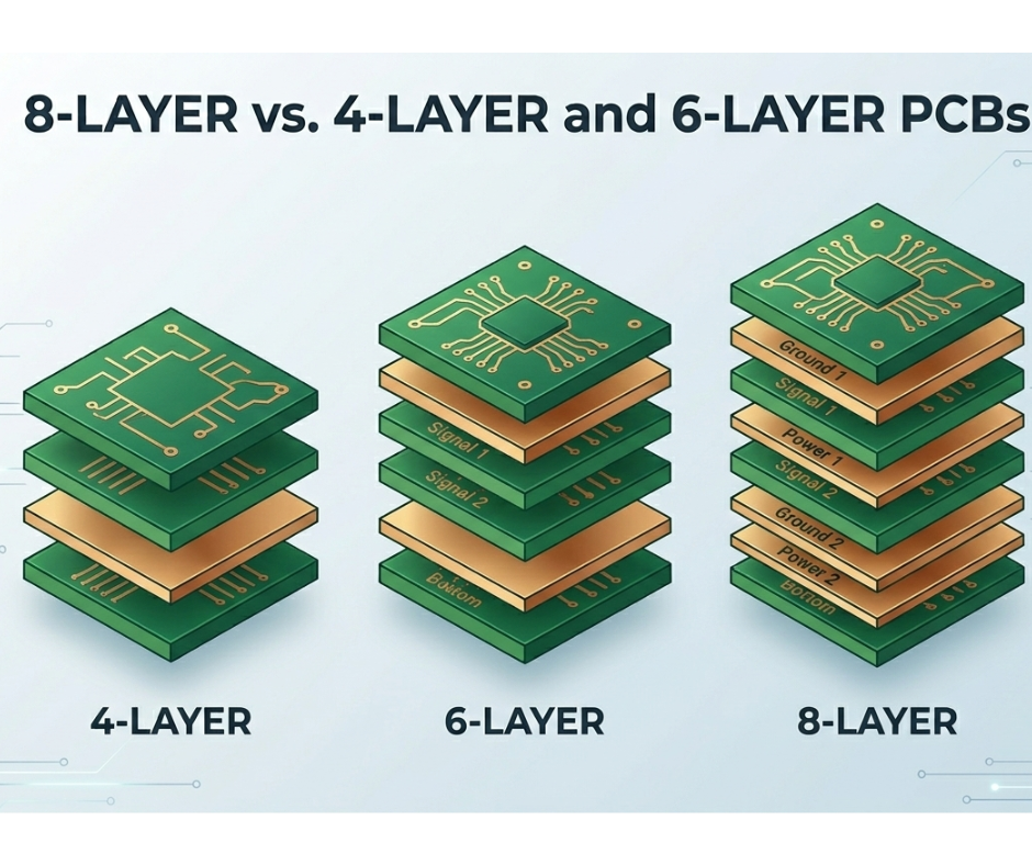
An 8-layer stackup adds a second dedicated ground plane and a second inner signal layer. That extra ground plane is what enables the tight EMI suppression, 15-20dB reduction in electromagnetic radiation, and impedance control accuracy within plus or minus 5% that high-speed digital systems:
- DDR4/5
- PCIe Gen 3+
- GigE
- 28Gbps+ signals
These are demands to pass EMC certification.
The practical threshold: if your design runs high-frequency circuits above 1GHz, carries high-speed differential pairs like USB, HDMI, or PCIe, or operates in a high-EMI environment, you need 8 layers. Below that, 6 layers likely suffices and costs less.
8-Layer PCB Stackup Design
Standard 8-Layer Stackup Configuration
A standard 8-layer stackup uses 1 oz copper per layer across all eight layers — the 1/1/1/1/1/1/1/1 oz configuration. Outer layers run at base copper thickness plus plating copper. Inner layers typically start at 0.5 oz before plating. This matters because uneven copper distribution across layers causes warpage during lamination.
Good fabs balance copper fill across all layers, sometimes adding non-functional copper pours in sparse areas. Ask specifically how the fab manages copper balancing on asymmetric designs — a specific answer is a green flag; vagueness is not.
Standard board thickness for 8-layer builds runs 1.6mm for general electronics, 2.0mm for industrial applications, and 2.4mm for power-heavy designs. Confirm thickness with your fab before finalizing Gerbers.
Prepreg and Core Material Selection
1. Why High-Tg FR-4 is the Baseline
Standard FR-4 softens during the lead-free reflow peak. Specifying Tg170 prevents via barrel cracking and the latent intermittent openings that characterize 8-layer board fatigue.
2. High-Frequency Dielectrics

For designs exceeding 1GHz, generic laminates fail. Applications requiring stable dielectric constants and low loss tangents must mandate specialty materials like Rogers 4350B, Arlon, or Taconic to ensure signal integrity across temperature swings.
3. The Prepreg Substitution
Fabs may quietly swap specified prepreg grades to reduce costs. A 15–30 micron shift in dielectric height can alter controlled impedance by up to 15%, causing system-level failures despite passing flying probe tests.
4. Product-Specific Stackup Verification
Move beyond generic thickness specs. Your procurement checklist must require named product codes on the stackup drawing.
5. Enforcing Material Compliance via Certification
Mandate that any material substitution requires written approval prior to lamination. Validating the build requires matching the physical Material Discovery Certificates against the approved engineering file to prevent “silent” shop-floor optimizations.
Impedance Control in the Stackup
Controlled impedance distinguishes a working 8-layer board from a failed board. For instance, the former passes inspection, while the latter fails in the field. For high-speed designs, it is better to aim for 50 ohms for single-ended signals, 90 ohms for USB differential pairs, 100 ohms for PCIe, Ethernet, and HDMI.
This manufacturing tolerance is usually plus or minus 10 per cent; critical nets are plus or minus 5 per cent, and these nets demand an alternative process strategy by the fab.
The 8-Layer PCB Manufacturing Process, Step by Step
Understanding each step lets you ask better questions during audits, catch problems at first article inspection, and write purchase orders that close the gaps fabs exploit.
Step 1: Design File Preparation and DFM Review
Production starts with your Gerber files: copper layers, drill data, solder mask, silkscreen, and board outline. A legitimate fab runs a Design for Manufacturability review before releasing to production:
- Checking minimum trace and space rules
- Annular ring dimensions
- Hole-to-copper clearances
- And aspect ratios against their actual process capabilities.
A fab that has never pushed back on a design with a DFM comment optimizes for speed at your expense.
Step 2: Material Preparation and Inner Layer Imaging
The fab cuts copper-clad laminate to panel size, applies photoresist, exposes it through a photomask under UV light, then etches away unwanted copper to form the inner layer circuit patterns. Precision at this stage determines registration quality across the entire stackup. Misalignment here compounds through every subsequent layer — it does not self-correct.
Step 3: Automated Optical Inspection of Inner Layers
AOI compares each etched inner layer against your Gerber data and flags shorts, opens, and copper anomalies. This step runs before lamination for one reason: once you laminate the layers, inner layer defects become permanent and invisible. Fabs that skip or sample inner layer AOI gamble with your yield. Ask specifically whether AOI runs 100% coverage on inner layers for your stackup type.
Step 4: Layer Stackup and Lamination
Lamination is where 8-layer manufacturing earns its complexity premium. Inner layers undergo oxide or alternative oxide treatment to improve adhesion to prepreg. Then the full stackup assembles:
- copper foil, prepreg
- core, prepreg
- core
Each layer precisely registered using optical punch alignment or X-ray targets — then pressed in a hydraulic lamination press under controlled heat and pressure profiles.
Step 5: Drilling — Mechanical and Laser
After lamination, the fab locates X-ray registration targets and begins drilling. Through-hole vias penetrate all eight layers. Blind vias connect an outer layer to specific inner layers. Buried vias connect inner layers only and sit invisible from both surfaces. Laser drilling creates microvias for HDI designs with ultra-dense BGA routing.
Via aspect ratio — board thickness divided by hole diameter — directly predicts plating difficulty. Beyond 10:1, copper plating in the barrel becomes unreliable and void risk rises sharply. Advanced fabs advertise up to 16:1 aspect ratio capability, but capability claims need coupon cross-section data to verify. High-aspect-ratio buried and blind vias on rushed jobs are where marginal fabs fail most consistently.
Step 6: Plated Through-Hole and Copper Plating
Chemical copper deposition seeds the hole walls, followed by electroplating to build copper to finished thickness. IPC minimum for plated through-hole copper is 25 microns average, 20 microns minimum.

Fabs under-plate barrel walls to speed up plating bath cycles — the boards pass initial electrical testing and fail under thermal cycling in the field. Cross-section your first article to verify plating thickness directly. That single step catches the most common hidden defect in overseas 8-layer production.
Step 7: Outer Layer Imaging and Etching
Outer layer imaging mirrors the inner layer process on the fully laminated board: dry film photoresist application, UV exposure, development, selective etching. What comes off the etching line determines your trace geometry and, in turn, your final impedance values.
Etch compensation — widening traces slightly to account for side-etch during etching — is standard practice at competent fabs. If a fab cannot explain how they apply etch compensation for your trace widths, your controlled impedance results will drift.
Step 8: Solder Mask Application
The fab applies LPI solder mask, exposes and develops it to open pads and vias, then UV cures the coating. IPC-SM-840 compliance governs solder mask performance. Color options — green, black, blue, red — do not affect electrical performance, but black solder mask makes visual inspection harder during assembly. Specify based on your assembly requirements.
Step 9: Surface Finish
ENIG is the standard surface finish for most 8-layer applications. It delivers flat, solderable, oxidation-resistant pads suitable for fine-pitch BGAs and high-reliability assemblies. HASL works for cost-sensitive designs without fine-pitch components. Immersion Silver, Immersion Tin, and OSP suit specific applications. ENEPIG adds a palladium layer between nickel and gold for applications requiring wire bonding alongside soldering.
Steps 10 and 11: Silkscreen and Board Profiling
Silkscreen printing adds component reference designators and board markings via inkjet or screen printing. CNC routing or V-scoring singulates individual boards from the panel. V-scoring on 8-layer multilayer boards introduces stress at the cut line.
In thermally cycling or vibrating environments, that stress creates micro-cracks — moisture ingress paths that drive conductive anodic filament growth between layers. Ask your fab explicitly which de-panelization method they use for your board dimensions and what their anti-CAF process controls include.
The Field Failure Standard Procurement Checklists Miss Entirely
Here is the failure that changed how this author audits 8-layer programs.
1. Why IPC Class 3 Isn’t a Field Guarantee
Standard checklists rely on certifications like IPC Class 3 or ISO 9001. However, as your case shows, a board can meet every static as-built specification while harboring latent defects. Procurement often mistakes a self-declaration of quality for a process-specific validation of high-stress environments.
2. Risks of De-panelization
Checklists verify CAF-resistant laminate but ignore the mechanical separation method. While V-scoring is cost-effective, the stress risers it introduces can negate high-end material properties. Audits must shift from What materials were used? to How was the finished assembly physically handled?
3. Thermal Cycling vs. Static Testing
Flying probe and AOI only catch “infant mortality” defects. They cannot predict how micro-cracks from de-panelization will propagate under 60°C temperature swings. A procurement checklist that misses Environmental Stress Screening data is essentially flying blind regarding field longevity.
4. The Tier 2 Disconnect
The failure stemmed from using standard procurement signals for a high-reliability robotics application. This heading addresses the need for application-specific auditing—where the checklist changes based on the vibration and moisture profiles of the end-use environment.
5. Hidden Costs of the Unit Price
Your case highlights that a 3x loss on warranty repairs dwarfs any initial savings from a cheaper fab or simplified de-paneling. Headings here should focus on Total Cost of Ownership modeling, moving procurement from “price per board” to “cost per deployed year.”
Via Types in 8-Layer PCB Manufacturing
Through-Hole Vias
Through-hole vias penetrate all eight layers and connect any layer to any other. They require one drilling and one plating operation, making them the most cost-effective interconnect. Use them as your default unless routing density forces otherwise.
Blind and Buried Vias
Blind vias connect an outer layer to one or more inner layers without full penetration. Buried vias connect inner layers only and stay invisible from both surfaces. Both types require additional lamination cycles, which multiplies process complexity and cost.

More critically: many overseas fabs that claim blind and buried via capability route these orders to lower-volume lines without the same process controls as their standard multilayer lines. Yield drops on complex blind buried designs at mid-tier fabs — ask for yield data on your specific via configuration before committing volume.
Microvias and Via-in-Pad
Microvias — laser-drilled holes under 150 microns — enable HDI designs and fine-pitch BGA routing. Via-in-pad places the via directly beneath a component pad to save routing space, but requires filling and capping the via to prevent solder wicking during assembly.
Ask which laser drill equipment the fab operates and what their microvia registration tolerance is. This separates advanced fabs from volume shops faster than any certification audit.
Materials Used in 8-Layer PCB Manufacturing
Substrate Materials
High-Tg FR-4 is the baseline for 8-layer boards entering lead-free assembly or harsh environments. For signal frequencies above 1GHz, specify Rogers 4350B, ARLON 85N, or TACONIC TLX for lower dielectric loss and stable Dk across temperature.
Ceramic and metal-core substrates handle high-power thermal management applications. Any time you see a fab quoting standard FR-4 for an 8-layer board going into a thermally demanding application, push back.
Copper Foil Grades
Standard electrolytic copper covers the majority of 8-layer designs. Designs running above 10GHz benefit from reverse-treated foil or very-low-profile copper, which reduces surface roughness and limits signal loss at high frequency. This specification only matters at high frequencies — but if it matters for your design, confirm the fab stocks it, because many do not carry RTF routinely.
Prepreg Options
Shengyi S1000HB is the most widely used high-reliability prepreg in Chinese fabs. Isola 370HR is standard in North American and European supply chains. The prepreg must match the core material’s coefficient of thermal expansion.
Mismatched CTE between prepreg and core creates delamination risk under thermal stress. This is why accepting generic equivalent material substitutions without engineering review is not acceptable on any 8-layer program.
The One Question Procurement Managers Never Ask
After years of watching procurement teams evaluate overseas PCB manufacturers, one question almost never appears during RFQ or audit:
“Can you show me your last three months of inner-layer registration data logs from your optical punch or X-ray, including scrap rates broken down by stackup type?”
1. Statistical Process Control
This heading addresses the psychological and operational divide between fabs. A procurement checklist must distinguish between a facility that monitors real-time data and one that relies on best-case projections. It highlights the importance of asking for raw SPC charts rather than curated summary reports.
2. The Registration Tolerance
A claimed 75 mm tolerance is meaningless without context. This section explores how average registration numbers hide the outliers that cause intermittent shorts in high-density 8-layer builds. It forces a technical audit of the fab’s automated optical alignment capabilities.
3. Yield Transparency
Standard reports often bury 8-layer scrap rates within general yield data. This heading exposes the practice of hiding failures in “rework” categories, which obscures the true stability of a production line and prevents accurate risk assessment for complex stackups.
4. Tier-1 Reality vs. Mid-Tier Marketing
There is a documented “yield gap” between Tier-1 automotive-grade fabs and mid-tier regional suppliers. By contrasting the 90–95% yield of high-end facilities against the true 75–85% yield of budget options, this section provides a framework for evaluating the effective unit cost.
5. Aspect Ratios and Impedance Control
Technical complexity scales non-linearly. This heading focuses on how specific design requirements. It explains why a standard procurement checklist fails when it treats all 8-layer designs as commodities.
The Person Who Actually Controls What Happens to Your Order
1. Sales Reps vs. Workshop Directors
Negotiations typically end with sales staff, but technical execution rests with the production manager. This heading highlights why price and lead time discussions are decoupled from actual floor priority, line loading, and equipment calibration.
2. Who Decides Your Queue Priority?
In high-capacity environments, the Workshop Director determines which orders get the primary lamination press and which wait for Monday. Establishing a direct technical link here ensures your 8-layer builds aren’t sidelined when production capacity tightens.
3. Meeting the Production Lead
Standard audits focus on the Quality Manager, yet the production team controls the variables that create quality. This section advocates for direct contact with the shop floor to bridge the gap between theoretical on-paper processes and real-time operator assignment.
4. Real-Time Risk Mitigation
Using your case study of the Guangdong lamination void, this heading illustrates how direct relationships bypass the 24-hour delay of sales-rep-only communication. It demonstrates how immediate technical feedback—such as receiving defect photos at midnight—can save a product launch deadline.
5. Practical vs. Theoretical Oversight in 8-Layer Programs
This concludes that the difference in output is concrete: a direct line to the person controlling the press translates to overnight reworks rather than two-week delays. It moves procurement from “managing a contract” to managing the manufacturing reality.
What This Means for Your Next Evaluation
8-layer PCB manufacturing complexity is real. Mid-tier overseas fabs optimize for throughput, not your reliability. Evaluate process evidence — inner-layer registration logs, cross-section plating data, named prepreg specs, real yield numbers. Build relationships inside the factory, not just with the sales team. The procurement decisions that skip this work show up as field failures, not line items on a quote.