PCB stack-up

Figure 2 Standard 8 layer stack up configurations

8-Layer PCB Design Guide: Stack-up, Applications, and Cost Analysis

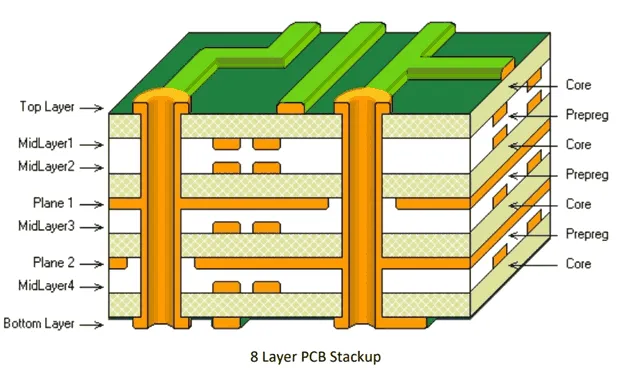
When your electronic design pushes beyond the limits of 6-layer PCBs, you need 8-layer printed circuit boards. An 8-layer PCB comprises of eight conductive copper layers separated by dielectric materials, providing higher signal integrity, electromagnetic shielding and power distribution. These multilayer boards are important for high-performance computing, telecommunications, advanced automotive systems, and aerospace applications where […]

8-Layer PCB Design Guide: Stack-up, Applications, and Cost Analysis Read More »

Type 1 standard 6-layer PCB stack-up configuration diagram

6 Layers PCB Manufacturing: Advanced Stack-up, Design Guidelines, and Cost Analysis

In the developing landscape of modern electronics, 6 layers printed circuit boards (PCBs) represent a critical advancement in multilayer PCB technology. A 6-layer PCB consists of six conductive copper layers separated by insulating dielectric materials, forming a complex sandwich structure that enables superior electrical performance and enhanced functionality. These boards occupy a strategic position in

6 Layers PCB Manufacturing: Advanced Stack-up, Design Guidelines, and Cost Analysis Read More »

image 1

PCB Stack-Up Design for 5G Applications: Layer Configuration and Grounding 

1. Introduction  1.1 The 5G Revolution and PCB Challenges  The global rollout of 5G wireless technology represents the most significant  transformation in telecommunications infrastructure since the advent of 4G LTE.  Operating across two distinct frequency bands sub-6 GHz for broad coverage and  millimeter wave (mmWave) frequencies ranging from 24 to 77 GHz for ultra-high  speed

PCB Stack-Up Design for 5G Applications: Layer Configuration and Grounding  Read More »