When your electronic design pushes beyond the limits of 6-layer PCBs, you need 8-layer printed circuit boards. An 8-layer PCB comprises of eight conductive copper layers separated by dielectric materials, providing higher signal integrity, electromagnetic shielding and power distribution. These multilayer boards are important for high-performance computing, telecommunications, advanced automotive systems, and aerospace applications where 6-layer designs cannot deliver the required performance.
This comprehensive guide facilitates you understand when to enhance from 6-layer to 8-layer PCBs, how to optimize your stack-up configuration, design for high-speed signals, control costs, and ensure manufacturing quality. Whether you design servers, 5G infrastructure, or autonomous vehicle controllers, this article provides the technical knowledge you need.
What is an 8-Layer PCB and When Do You Need It?
An 8-layer PCB is made up of eight conductive copper layers stacked with insulating dielectric materials between them. You organize these layers as signal layers, ground planes, and power planes. The copper layers offer tracks for signals and power, while ground planes provide return paths and electromagnetic shielding.
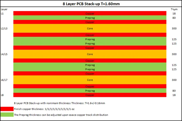
The standard 1.6mm thick 8-layer printed circuit board includes multiple cores and prepreg materials merged during lamination. You configure the layer stack-up based on your specific signal integrity, power distribution, and EMI requirements. Each design choice affects performance, so you need carefully plan your layer arrangement before manufacturing.
When to Upgrade from 6-Layer to 8-Layer
You should upgrade from 6-layer to 8-layer PCBs when you face these challenges:
- High-speed signal requirements: Your design uses DDR5 memory, PCIe Gen 4/5, or 100G Ethernet that demands better signal integrity than 6-layer can provide
- Complex power distribution: You need multiple voltage domains (3.3V, 5V, 12V, 1.8V, 1.2V) with dedicated power planes for clean power delivery
- Routing density: Your component placement requires more routing space than 6 layers can accommodate
- EMI control: You must meet strict electromagnetic compatibility standards that require additional ground planes
- Signal speeds above 10 Gbps: Your high-speed serial links need stripline routing with dual reference planes
- Thermal management: Additional copper layers help spread heat from power-hungry components
Standard 8-Layer PCB Stack-up Configurations
Your stack-up configuration determines signal quality, power integrity, and EMI performance. You must choose the arrangement that matches your design requirements. Following are three major 8-layer stack-up types:
Type 1: Balanced Stack-up (Most Common)
This is the most used 8-layer configuration for general-purpose applications. You get excellent signal integrity with good power distribution:
- Layer 1: Top Signal (Component Side)
- Layer 2: Ground Plane (GND)
- Layer 3: Signal Layer (High-Speed)
- Layer 4: Signal Layer (High-Speed)
- Layer 5: Ground Plane (GND)
- Layer 6: Signal Layer
- Layer 7: Power Plane (VCC)
- Layer 8: Bottom Signal (Solder Side)
This stack-up gives you two ground planes (L2, L5) that sandwich your essential high-speed signals on L3 and L4. You route these signals as strip lines with excellent EMI shielding. The power plane on L7 provides stable voltage distribution close to the bottom components.
Type 2: Multiple Ground Planes (High-Speed Digital)
For designs with DDR5, PCIe Gen 5, or 100G Ethernet, you need highest EMI shielding. This configuration offers three or four ground planes:
- Layer 1: Top Signal
- Layer 2: Ground Plane
- Layer 3: High-Speed Signal (Stripline)
- Layer 4: Ground Plane
- Layer 5: Power Plane (can be split for multiple voltages)
- Layer 6: Ground Plane
- Layer 7: High-Speed Signal (Stripline)
- Layer 8: Bottom Signal
You get four ground planes (L2, L4, L6) that provide superior return paths and EMI shielding. Your high-speed differential pairs on L3 and L7 run between ground planes as striplines. This configuration minimizes crosstalk and ground bounce, essential for signals above 10 Gbps.
Type 3: Mixed-Signal Design
When you combine sensitive analog circuits with noisy digital logic, you need physical separation:
- Layer 1: Mixed Signal (Digital + Analog sections)
- Layer 2: Ground Plane (Split: Digital GND / Analog GND)
- Layer 3: Digital Signal Layer
- Layer 4: Digital Signal Layer
- Layer 5: Analog Signal Layer
- Layer 6: Ground Plane (Split: Digital GND / Analog GND)
- Layer 7: Power Plane (Split: Digital VCC / Analog VCC)
- Layer 8: Mixed Signal
You separate digital circuits (L3, L4) from analog circuits (L5) with split ground and power planes. This prevents digital switching noise from coupling into sensitive analog signals.
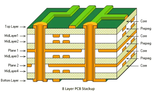
Figure 2 Standard 8-layer stack-up configurations
8-Layer vs 6-Layer vs 10-Layer PCB: Performance Comparison
Choosing the right layer count affects your design performance, cost, and manufacturability. This comparison helps you make informed decisions:
| Factor | 6-Layer | 8-Layer | 10-Layer |
| Signal Integrity | Good (up to 5 Gbps) | Excellent (up to 25 Gbps) | Superior (>25 Gbps) |
| Power Planes | 1-2 planes | 2-3 planes | 3-4 planes |
| EMI Performance | Good | Excellent | Superior |
| Routing Density | High | Very High | Maximum |
| Relative Cost | Baseline | 1.3-1.5x | 1.5-2x |
| Lead Time | 10-15 days | 12-18 days | 15-20 days |
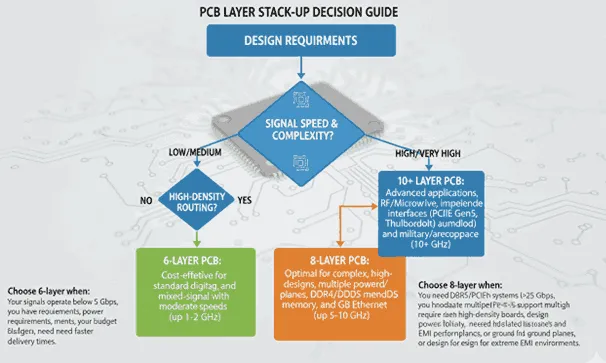
When to Choose Each Option
Select 6-layer when: Your signals operate below 5 Gbps, you have moderate power requirements, your budget is constrained, and you need faster delivery times.
Select 8-layer when: You need DDR5/PCIe Gen 4-5 support, require multiple power domains, design high-density boards, need superior EMI performance, or operate signals between 5-25 Gbps.
Select 10-layer when: You design ultra-high-speed systems (>25 Gbps), need maximum routing flexibility, require multiple isolated power and ground planes, or design for extreme EMI environments.
Laminate Materials
You choose materials based on your electrical and thermal requirements:
- FR-4 Standard (TG130-150): Most economical for general applications
- High-TG FR-4 (TG170-180): Better thermal stability for lead-free soldering
- Rogers RO4003C/RO4350B: High-frequency materials for RF applications with stable Dk
- Hybrid constructions: FR-4 cores with Rogers prepreg for cost-performance balance
Board Thickness and Copper Weight
Standard 1.6mm thickness works for most 8-layer designs. You use 1oz copper (35µm) on outer layers for standard designs or 2oz (70µm) for high-current applications. Inner layers typically use 0.5oz or 1oz copper depending on signal or plane requirements.
Impedance Control Requirements
Impedance control is critical for 8-layer high-speed designs. You target 50Ω for single-ended signals, 90Ω for USB differential pairs, and 100Ω for PCIe, Ethernet, and HDMI. You work with your manufacturer to specify stack-up parameters (trace width, dielectric thickness) that achieve these targets within ±7-10% tolerance.
Primary Applications for 8-Layer PCBs
High-Performance Computing
You use 8-layer PCBs for server motherboards, workstation boards, AI/ML accelerator cards, and GPU boards with DDR5 memory. These applications require multiple power planes, excellent signal integrity for high-speed memory interfaces, and superior thermal management.
Telecommunications & Networking
100G/400G Ethernet switches, 5G base stations (gNB), baseband processing units, and optical transceivers all require 8-layer designs. You need strip line routing for high-speed differential pairs and multiple ground planes for EMI control.
Advanced Automotive Systems
Autonomous driving ECUs, advanced ADAS systems, high-performance infotainment, and EV power electronics controllers use 8-layer PCBs. You must meet strict automotive EMC standards (CISPR 25) and operate across wide temperature ranges (-40°C to +125°C).
Aerospace & Defense
Avionics systems, radar and RF systems, and ruggedized military equipment require 8-layer construction for reliability, EMI shielding, and performance in harsh environments.
Advanced Design Guidelines for 8-Layer PCBs
Power Distribution Network (PDN) Design
You design your PDN with multiple voltage rails, proper decoupling strategy (0.1µF, 1µF, 10µF, bulk capacitors), and power plane partitioning. You place decoupling capacitors close to IC power pins with short via paths to minimize inductance. You use power plane analysis tools to verify your PDN impedance stays below target values across your frequency range.
Via Strategy and Back-drilling
You use through-hole vias for most connections. For signals above 10 Gbps, you must back-drill via stubs to eliminate resonance. You consider blind/buried vias for high-density BGA fan-outs. You add ground stitching vias (every 1000-2000 mils) around board edges and near high-speed components for EMI control.
Signal Integrity Best Practices
You route high-speed signals as striplines between ground planes. You match differential pair lengths within 5 mils and maintain consistent spacing. You avoid vias in differential pairs when possible. You provide continuous return paths and avoid crossing split planes. You use proper termination (series, parallel, or AC) based on your signal characteristics.
EMI Control Techniques
You maintain solid ground planes with minimal disruption. You use edge radiation control with ground via fencing. You properly manage split planes with deliberate connections. You route clock and high-speed signals on inner stripline layers for maximum shielding.
Manufacturing Capabilities & Technical Specifications
Modern PCB manufacturers offer advanced capabilities for 8-layer boards:
| Specification | Capability |
| Min Trace/Space | 3mil/3mil (advanced), 4mil/4mil (standard) |
| Via Types | Through-hole, Blind (L1-L4, L5-L8), Buried (L2-L7) |
| Impedance Tolerance | ±7-10% with TDR testing |
| Surface Finish | HASL, ENIG, OSP, Immersion Silver/Tin |
Via Technology Options
Through-hole vias work for most 8-layer connections. You add blind vias (adds 20-30% cost) for dense BGA fan-outs. You use buried vias (adds 30-40% cost) only when routing density demands. You specify back-drilling for signals above 10 Gbps to remove via stubs.
Cost Factors: Understanding 8-Layer PCB Pricing
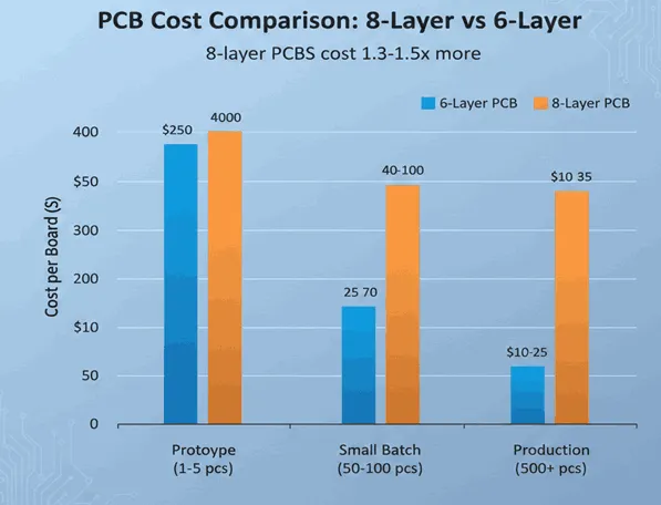
Cost Comparison: 8-Layer vs 6-Layer
8-layer PCBs cost 1.3-1.5x more than 6-layer boards. Prototype pricing: 8-layer $200-400 per board vs 6-layer $150-300. Production (500+ pcs): 8-layer $10-35 per board vs 6-layer $8-25. The premium pays for additional layers, more complex processing, and longer manufacturing time.
Factors Affecting 8-Layer PCB Cost
- Quantity: Larger orders significantly reduce per-unit cost through panel optimization
- Via technology: Blind/buried vias add 20-40% cost over standard through-hole
- Materials: Rogers high-frequency materials cost 2-4x more than standard FR-4
- Impedance control: TDR testing adds $100-300 per design but ensures performance
- Back-drilling: Adds cost but essential for >10 Gbps signals
- Board size: Efficient panel utilization reduces waste and cost
- Lead time: Standard 12-18 days vs expedited 5-7 days (+40-80% premium)
Cost Reduction Strategies
- Use standard 1.6mm thickness and 1oz copper when possible
- Avoid blind/buried vias unless routing density demands
- Optimize board dimensions for efficient panel utilization
- Choose standard FR-4 unless high-frequency materials are required
- Accept standard lead times—rush charges add 40-80% to cost
- Work with manufacturer DFM review to identify cost savings early
Quality Control and Testing for 8-Layer PCBs
Electrical Testing
Every 8-layer board undergoes electrical testing to verify continuity and isolation. Flying probe testing works for prototypes and small batches. Fixture-based testing (bed of nails) is more efficient for production volumes.
Impedance Testing (TDR)
Time Domain Reflectometry (TDR) testing verifies your controlled impedance traces meet specifications. Test coupons are fabricated on production panels and measured. Results document actual impedance values, typically within ±7-10% of target. This testing is essential for high-speed designs and worth the additional cost.
Advanced Inspection Methods
Automated Optical Inspection (AOI) catches surface defects on outer layers. X-ray inspection is critical for 8-layer boards it verifies via formation, barrel plating quality, and layer-to-layer registration. Microsection analysis provides cross-sectional examination for first article inspection and qualification.
Pros and Cons Table of 8 Layer PCBs
Consider these advantages and disadvantages when choosing 8-layer PCBs:
| Advantages | Disadvantages |
| Superior signal integrity for high-speed designs (5-25 Gbps) | Higher cost (1.3-1.5x vs 6-layer) |
| Multiple power/ground planes for clean power distribution | Longer lead time (12-18 days) |
| Excellent EMI shielding with multiple ground planes | More complex design process |
| High routing density for complex designs | Requires advanced design tools and expertise |
| Supports DDR5, PCIe Gen 4/5, 100G Ethernet | Tighter manufacturing tolerances required |
Why Choose Wonderful PCB for 8-Layer PCB Manufacturing
Advanced Manufacturing Capabilities
Wonderful PCB operates state-of-the-art facilities for 8-layer PCB production. We support blind/buried vias, back-drilling for high-speed signals, and controlled impedance manufacturing with TDR verification. Our equipment maintains tight tolerances essential for 8-layer complexity.
Engineering Support
Our engineering team provides DFM (Design for Manufacturing) review to identify potential issues before production. We help optimize your stack-up configuration for your specific requirements. We offer impedance calculation assistance and signal integrity consultation to ensure your design meets performance goals.
Quality Assurance
Wonderful PCB maintains ISO 9001 certification and UL recognition. Every 8-layer board undergoes rigorous testing including electrical verification, impedance testing with TDR, AOI inspection, and X-ray verification of internal structures. We provide complete documentation including test reports and material certificates.
Competitive Pricing
FAQ
Q1: How much more expensive is 8-layer compared to 6-layer?
8-layer PCBs typically cost 1.3-1.5x more than 6-layer boards. For prototypes (10 pieces), expect $200-400 per board versus $150-300 for 6-layer. At production volumes (500+ pieces), 8-layer boards range from $10-35 versus $8-25 for 6-layer. The cost difference narrows at higher volumes.
Q2: Do I need blind/buried vias for 8-layer PCBs?
Not always. Most 8-layer designs use only through-hole vias successfully. You need blind or buried vias when you have extremely high routing density (fine-pitch BGAs), limited board space, or via-in-pad requirements.
Q3: What applications require 8-layer PCBs?
Server motherboards, AI/ML accelerator cards, 5G base stations, 100G Ethernet switches, automotive ADAS controllers, autonomous driving ECUs, aerospace avionics, and high-performance industrial controllers all typically use 8-layer construction for required performance and reliability.
Q4: Can 8-layer PCBs handle high-speed interfaces like DDR5 and PCIe Gen 5?
Yes, 8-layer PCBs are ideal for these interfaces. The multiple ground planes provide excellent return paths and EMI shielding. You route high-speed differential pairs as striplines between ground planes, achieving the signal integrity required for DDR5 (up to 6400 MT/s) and PCIe Gen 5 (32 GT/s).
Conclusion
8-layer PCBs provide the best solution for high-performance electronics that exceed 6-layer capabilities. You get excellent signal integrity for high-speed interfaces, multiple power and ground planes for clean power distribution, excellent EMI shielding, and high routing density for complex designs. While 8-layer boards cost more than 6-layer alternatives, the investment delivers measurable improvements in performance, reliability, and system capability.
Success with 8-layer designs needs careful stack-up arrangement, consideration to signal integrity rules, proper power distribution network design, and collaboration with an experienced manufacturer.
Ready to get started with your 8-layer PCB design? Contact Wonderful PCB today for a free quote, stack-up consultation, and DFM analysis. Our engineering team is ready to help you optimize your design for performance and manufacturability.
Get Your 8-Layer PCB Quote Today!
Email [email protected]| Phone: + 0086 0755-86229518
Visit: www.wonderfulpcb.com