Executive Summary
A regional retail chain needed a PCI-certified, EMVCo-compliant Android tablet for branch-level payment processing. What followed was a $280,000 hardware failure, an 11-week re-spin, and lessons most OEM brochures won’t document. This case study covers the architecture decisions, the failure, the fix, and the security engineering realities that separate a financial tablet from a device that merely passed its certification audit.

What Banks Think They’re Buying
The truth we tell every client before touching a schematic: PCI PTS, EMVCo L1/L2, Android Enterprise, and MDM compliance are not a security guarantee. They are a liability transfer mechanism.
Also read: Rugged Tablet Case Study
PTS certification is a snapshot, not a shield. PCI PTS v6 certifies the device at a fixed point in time. Any firmware update — including a security patch — triggers re-certification. Most OEMs lock firmware to avoid re-cert costs. Banking tablets routinely run 18–24 months behind on Android security patches. The device is “PCI compliant.” The kernel is unpatched. Those two facts coexist until a breach forces the conversation.
Android Enterprise with full MDM kills offline deployments. The standard stack assumes constant cloud connectivity. In low-connectivity environments, our data shows a 30–40% higher field failure rate versus locked AOSP builds. Devices brick on nightly reboots when MDM can’t phone home.
Buyers think they are buying safety. They are actually buying lock-in and future re-cert pain.
Client Requirements & Why Standard Tablets Fail in Banking
What the Client Asked For
The brief was standard for a financial-grade Android tablet for banking:
- 10-inch FHD IPS display for in-branch customer onboarding
- Integrated NFC reader, smart card reader, high-resolution front camera for eKYC tablet hardware workflows
- LTE/5G connectivity, hardware-level encryption, secure boot
- PCI DSS + EMV tablet integration, 5+ year production lifecycle
The Compliance Checklist (And What It Doesn’t Cover)
- PCI DSS 4.0.1 — Requirement 6.4.3 keeps the buyer liable for third-party code even on a “compliant” device
- EMVCo L1/L2 — certifies contactless performance in controlled lab conditions, not real-world EMI from metal shelving or motors
- CE / FCC — says nothing about firmware supply-chain integrity or zero-day kernel exposure
- Android Enterprise Recommended — requires Google Play Services; incompatible with offline-first architectures
- Regional telecom certification — adds 4–8 weeks to PVT in most APAC and MENA markets
The certification map does not match the territory. That gap is where most banking tablet development projects fail.
System Architecture & SoC Selection
Why We Chose Qualcomm Over MediaTek
SoC selection for a financial tablet is a lifecycle decision, not a benchmark decision. We evaluated both platforms against four criteria:
- TEE quality — GlobalPlatform API compliance, third-party security lab validation depth
- Lifecycle availability — financial hardware needs a 5–7 year supply window; consumer MediaTek SKUs don’t carry that guarantee
- Android upgrade path — a SoC that loses kernel support mid-deployment forces re-cert on the buyer
- Crypto acceleration — hardware-accelerated encryption is the difference between 9 hours of battery life and 6 under financial workload
For offline-first deployments, this calculus shifts — covered in the software section below.
Hardware Block Architecture
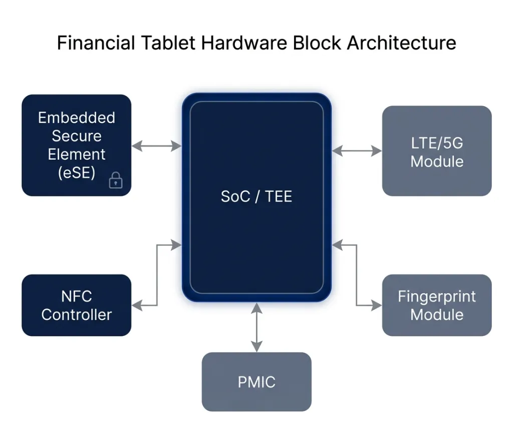
The subsystem integration for a secure Android tablet OEM project involves interdependencies most block diagrams hide:
- SoC → TEE lives here; drives all subsystems
- Embedded Secure Element (eSE) → isolated from main AP; EMV cryptographic operations and payment key storage
- NFC controller → interfaces directly with eSE; antenna placement here is where most teams get into trouble
- Fingerprint module → biometric eKYC; requires secure channel to TEE
- LTE/5G module → RF antenna must be isolated from NFC antenna to prevent interference
The integration risk is in the interactions, not the components.
Security Engineering: Hardware, Firmware & OS
TEE, Secure Boot & Real Attack Scenarios
Three threat scenarios shaped our security architecture for this banking Android tablet:
Firmware tampering — attacker with physical access flashes modified firmware bypassing payment integrity checks. Defense: verified boot chain anchored in hardware; any break halts boot entirely.
NFC relay attacks — in high-density retail with multiple readers within 30cm, passive attackers can attempt relay intercepts. Defense: all payment operations execute inside the eSE; the payment key never reaches the main application processor.
Device theft mid-session — Defense: hardware-backed keystore with biometric binding; MDM-compatible remote wipe with TEE-enforced lock that survives OS reflash.
Secure Element & NFC Payment Encryption
The embedded secure element handles three functions that cannot be delegated to software: EMV cryptographic operations, payment key storage (keys never exist in plaintext outside the eSE), and NFC transaction isolation where the eSE communicates directly with the NFC controller, bypassing the AP entirely. This is what makes a secure payment tablet architecturally different from a consumer device with a payment app.
OS-Level Lockdown
- Kiosk mode — single-application lock; no access to settings, app drawer, or browser
- Restricted permissions — NFC and camera accessible only to the verified payment application
- MDM compatible banking tablet — remote lock, wipe, and audit trail for compliance reporting
The detail beginner guides never mention: TEE key provisioning must use a factory-fresh, device-unique attestation chain — never re-used development keys. Dev keys burned into EVT units for testing convenience, if not explicitly replaced at PVT, cause remote attestation to fail silently in the field. The device passes every lab test and is cryptographically unverifiable post-deployment.
PCB & PCBA Engineering for Financial Reliability
The Failure That Cost $280,000
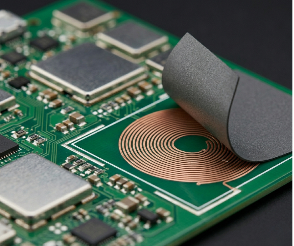
In a 2024–2025 production run, we placed the NFC antenna directly over the battery pack — standard smartphone layout. The Qualcomm NFC controller and eSE combination was proven. The DVT enclosure was plastic. We ran 10,000 tap cycles. We passed EMVCo lab certification. DVT sign-off was clean.
PVT told a different story.
The first 800-unit production run went into actual stores — metal shelving, refrigeration motors, multiple NFC readers in proximity. Field failure rate: 22%. Nearly one in four transactions timing out.
Root cause: the final metal chassis, battery swell under real operating cycles, and a 0.8mm adhesive tolerance shifted the NFC antenna’s resonant frequency by approximately 350 kHz — enough to drop the coupling coefficient below the ISO 14443 minimum in marginal reader fields. The antenna was tuned for a plastic prototype. Production killed it.
The fix: new PCB revision with tunable impedance matching network, dedicated ferrite shield, and metal keep-out zone. 11 weeks. ~$280,000 in NRE, scrap, and expedited re-certification. The first-year volume contract was lost.
“Lab equals plastic prototype. Production equals metal plus tolerances. They are different animals.”
NFC Antenna Placement: The Rule That Doesn’t Appear in Guides
Our protocol after that failure, now non-negotiable: rear cover placement, minimum 8–10mm offset from the battery pack, dedicated metal keep-out zone. Even 1mm closer, or adhesive or paint variance in production, kills the Q-factor enough to produce intermittent failures that pass DVT and fail in stores.
Two solutions for production variance: a tunable matching network (costs more upfront) or over-designed field strength (trades EMI compliance headroom). No clean answer — only managed trade-offs. Teams that copy smartphone antenna layouts discover this in PVT, not before.
Multi-Layer PCB Design for Financial-Grade NFC
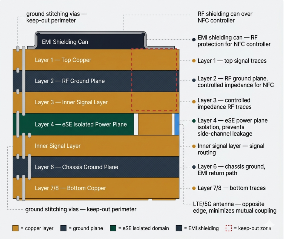
- 6–8 layer stack — controlled impedance for RF traces; >10% deviation measurably affects NFC coupling distance
- EMI shielding — RF cans over the NFC controller, ground stitching vias along the keep-out perimeter
- eSE power plane isolation — dedicated ground pour prevents side-channel leakage through AP power noise
- Antenna separation — NFC and LTE/5G antennas on opposite device edges to minimize mutual coupling
Financial environments are hostile RF environments. The secure tablet PCB design is optimized for the store, not the lab.
Field Readiness: Durability & Financial Device Power Management
Built for Daily Commercial Use
Financial tablets aren’t rugged industrial hardware, but they face daily punishment. Non-negotiables:
- 1-meter drop compliance — branch staff drop devices
- 10,000+ USB insertion cycles — a port that fails at 3,000 cycles on a 5-year lifecycle device is a field service problem
- Matte, slim, professional finish — customer-facing hardware that needs to look credible through years of handling
The Battery Reality Nobody Puts in the Brochure
Spec sheets claim 12–15 hours on an 8,000 mAh cell. Under real financial workload — full-disk encryption, continuous NFC polling, EMV transaction logging, TEE key operations — the real figure is 7–9.5 hours.
Why the gap: StrongBox and TEE secure processors cannot enter the same deep sleep states as the main AP during active key operations. That costs 15–25% additional drain versus a software keystore. In 24/7 kiosk deployments, buyers discover within 12 months they need external battery packs or a swap program. Plan for 8 hours under financial workload. If you need 12, plan for supplemental power.
Software Customization & Enterprise Integration
Android Enterprise — With One Critical Caveat
Android Enterprise is the right framework for always-online urban deployments: kiosk configuration, EMM integration, secure OTA updates with verified boot chain. The caveat is connectivity dependency — every element assumes reliable network access.
When to Drop Android Enterprise Entirely
For offline-first deployments with unreliable cellular and nightly power cuts, the standard stack was actively harmful. Devices bricked on reboot when MDM check-ins failed. TEE attestation refreshes drained batteries that couldn’t complete a charge cycle.
The architecture that shipped instead:
- StrongBox (SoC hardware keystore) replacing eSE — no TSM provisioning dependency
- HCE with acquirer-side tokenization under a CPoC model
- Local offline token cache with time-bound cryptograms; daily re-sync on connectivity return
- Locked AOSP — no Google Play Services, custom SELinux policy, verified boot only
Results: 30–40% lower BOM cost, 2× battery life offline, passed local central-bank certification and PCI CPoC. Trade-off: greater software complexity and heavier reliance on the acquirer’s token vault.
The standard stack is ideal for urban always-online banks. For offline-first deployments, it is the wrong starting point.
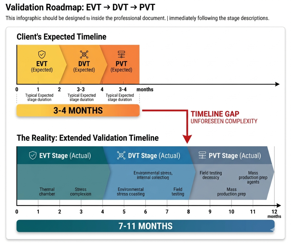
Validation Roadmap: EVT → DVT → PVT for Fintech Devices
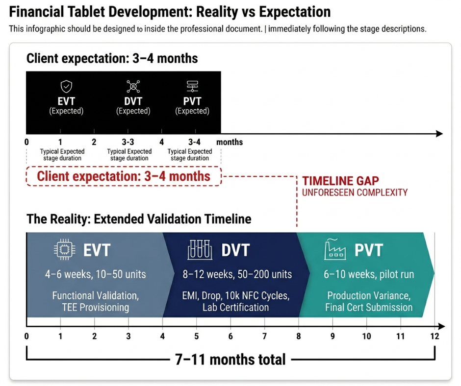
The largest expectation gap in financial tablet development: clients expect 3–4 months (smartphone timelines). Banking-grade hardware with PCI PTS, EMVCo, and custom TEE takes 7–11 months.
EVT — 4–6 weeks, 10–50 units: Functional validation, TEE provisioning, initial antenna behavior in real chassis. Surprises here are manageable — tooling not yet committed.
DVT — 8–12 weeks, 50–200 units: Full environmental testing: drop, EMI, thermal, battery cycles, 10,000+ NFC transaction suite. Third-party lab sign-off for EMVCo and PCI PTS. Any hardware change restarts portions of the lab queue.
PVT — 6–10 weeks, pilot production run: Where real production variance surfaces. DVT sign-off does not guarantee PVT success — the $280k failure above was DVT-clean and PVT-collapsed. Final re-submission adds 4–6 weeks for regional telecom approval.
Total: 7–11 months. Put this in the proposal. Clients who accept it are equipped to run the program.
Mass Production & Security-Controlled Manufacturing
SMT Assembly & Quality Control
- Fine-pitch BGA — 100% X-ray inspection on security-critical components; not sampling
- eSE traceability — every secure element serialized and tracked to its unit; chain of custody is a compliance requirement
- NFC antenna assembly — adhesive thickness is a controlled variable; assembly jigs enforce keep-out geometry
Security-Controlled Firmware Provisioning
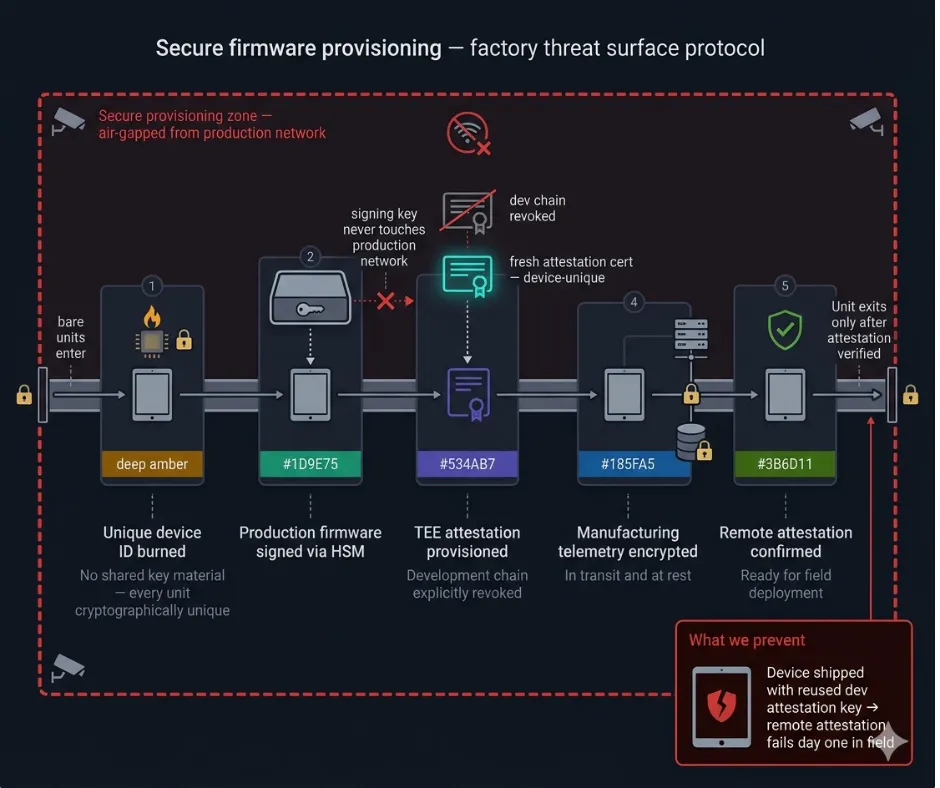
The factory floor is a threat surface. Our provisioning protocol:
- Unique device ID burned at factory — no shared key material origin
- Production firmware signed via HSM; signing key never touches the production network
- Fresh TEE attestation certificate per device; development chain explicitly revoked before the unit ships
- Manufacturing telemetry encrypted in transit and at rest
A device that passes every hardware test and ships with a re-used development attestation key fails remote attestation on day one in the field.
Key Engineering Challenges & How We Solved Them
| Challenge | Risk | Solution | Result |
| NFC antenna detuning at PVT | 22% field failure; $280k re-spin cost | Implemented tunable matching, 8–10mm offset, and strict keep-out zones. | Failure rate dropped from 22% to <3%. |
| Always-online MDM in offline markets | Device bricking; 30–40% higher failure rate | Transitioned to AOSP + StrongBox + HCE + CPoC architecture. | 2× battery life; 30–40% lower BOM costs. |
| 18–24 month patch lag | Unpatched kernel; false compliance status | OTA with TEE-verified signing + strict patch SLA in contracts. | Achieved robust, current security posture. |
| PVT yield collapse | 18% scrap/rework on the first lot | Introduced production chassis antenna testing pre-PVT. | <3% rework in all subsequent production runs. |
| CISO deal blockage | Pilots stalled for 6–12 months | Paid pilot + shared responsibility matrix + third-party pen-testing. | Significant acceleration in subsequent procurement cycles. |
The Real Stakeholders: Who Is Actually in the Room
The CISO is the hardest blocker. Official objection: “integration risk.” Actual fear: personal liability if a breach occurs on hardware they approved. They answer to the regulator. A certification document does not move this fear — a third-party penetration test report and explicit shared responsibility matrix do.
CTO / IT Operations worries about Android fragmentation. A contractual 5-year patch SLA answers the real question: what happens when the SoC loses Android support?
Procurement / CFO presents as a price objector. Real concern: hidden TCO — battery swap programs, re-cert costs, NFC field service. The ROI slide quantifies cash-handling cost reduction against full device lifetime cost.
Legal appears at contract stage with indemnity clauses most OEM agreements don’t cover. Budget time.
What actually closes a stalled deal: a 4–6 week paid pilot, 20–50 units, full transaction logging, shared responsibility matrix pre-agreed. Every stalled deal that moved forward did so after a pilot. It converts marketing claims into evidence.
What Is Coming in 24 Months: The Requirement Nobody Is Ready For
Based on live RFPs in early 2026 — not analyst forecasts — one requirement is appearing that most financial tablet OEM manufacturers are not equipped to meet.
Post-quantum cryptography is now a procurement line item.
Buyers are explicitly requiring NIST PQC algorithms — FIPS 203 (ML-KEM), FIPS 204 (ML-DSA), FIPS 205 (SLH-DSA) — in hardware and firmware for key exchange, signatures, and full-disk encryption. This follows CISA’s January 2026 guidance mandating PQC-capable products in federal endpoint security. Banks are watching federal procurement and copying the language into their own RFPs.
The stated driver: “harvest-now-decrypt-later” attacks, where financial data captured today is held for decryption once a cryptographically relevant quantum computer exists. Regulators are treating this as near-term operational risk, not a 2035 problem.
Alongside PQC: runtime side-channel anomaly detection inside the TEE — monitoring power, EM, and timing signatures during crypto operations to detect Rowhammer variants, clock glitching, and firmware implants.
The questions in live RFPs that didn’t exist in 2023: “Can the TEE attest PQC keys? What is your post-quantum migration timeline? Does the hardware root-of-trust support CRQC-resistant algorithms by 2028?”
Hardware platforms designed without PQC thermal and power headroom face a full redesign before 2028. The OEMs treating this as a 2027 problem will be on emergency timelines to meet certifications buyers are writing into contracts today.
Conclusion: What Secure Financial Tablet Development Actually Requires
The gap between a financial tablet that passes certification and one that performs in the field is not a hardware gap. It is an engineering culture gap.
Five things separate deployments that succeed from ones that don’t:
Architecture matched to deployment context — TEE + eSE + Android Enterprise for always-online urban banking; StrongBox + HCE + AOSP for offline-first. The auditor’s checklist is not the architecture brief.
NFC antenna as a first-order design constraint — the 8–10mm offset rule and metal keep-out zone are decided before PCB layout is committed, not after PVT yields collapse.
Honest validation timelines from day one — 7–11 months for a banking-grade device. That number in the proposal filters the wrong clients and builds credibility with the right ones.
Security-controlled manufacturing — fresh attestation keys per device, HSM-signed firmware, eSE chain of custody. The factory floor is part of the threat model.
A post-quantum roadmap already written — PQC is in live RFPs and CISA guidance. Any fintech tablet ODM that cannot articulate a migration path by 2026 will be re-specified before its production lifecycle ends.
The market is not short of vendors with a PCI certificate and a spec sheet. It is short of engineering partners who have run the program, absorbed the failures, and built those lessons into every project that follows.
FAQs
How long does banking-grade Android tablet development actually take?
The realistic EVT → DVT → PVT cycle is 7–11 months for devices requiring PCI PTS, EMVCo, and custom TEE certification. Clients expect 3–4 months based on smartphone timelines. The gap comes from mandatory third-party lab re-testing after any hardware revision.
What is the real battery life under financial workloads?
On an 8,000 mAh cell: 7–9.5 hours under sustained financial workload. Spec sheets cite 12–15 hours under consumer mixed use. StrongBox and TEE processors can’t deep sleep during active key operations — that costs 15–25% additional drain. Plan for supplemental power in kiosk deployments.
Is PCI PTS certification enough?
No. It certifies the device at one point in time. Subsequent firmware changes may require re-certification. It does not evaluate OS patch cadence, firmware supply-chain security, or ongoing TEE attestation health. Treat it as a baseline filter, not an ongoing guarantee.
When should we use HCE + StrongBox instead of an embedded secure element?
For offline-first deployments where TSM connectivity for eSE provisioning can’t be guaranteed. HCE with acquirer-side tokenization (CPoC model) delivers 30–40% lower BOM and 2× battery life offline, at the cost of greater software complexity and acquirer-side token vault responsibility.
Why is post-quantum cryptography appearing in RFPs now?
NIST finalized FIPS 203/204/205 and CISA issued PQC mandates in January 2026. Banks are incorporating these into procurement, citing “harvest-now-decrypt-later” attacks. Hardware without PQC support in the TEE faces redesign pressure before 2028.
What actually closes a deal with a bank’s security team?
The CISO’s real fear is personal liability. A third-party pen-test report, explicit shared responsibility matrix, and a 4–6 week paid pilot with 20–50 units convert OEM claims into evidence the security team can act on. Certifications alone don’t close these deals.