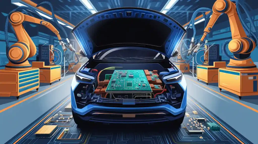
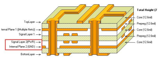
You cannot see inside multilayer printed circuit boards with your eyes. X-ray 3D imaging reveals hidden traces and vias that persist invisible to cameras and microscopes. Traditional reverse engineering needs destructive layer separation. You dissolve layers with chemicals, abolishing the original board permanently. Manual de-layering takes more time (weeks) and leaves you with nothing to verify your work against.
3D Imaging X-ray tomography provides non-destructive analysis of all internal Printed Circuit Board structures. The technology advanced from simple 2D X-ray inspection in early 2000s to sophisticated 3D CT scanning systems available in 2026. You preserve the original board completely intact. You see all layers simultaneously with micron-level resolution. Analysis that took weeks now completes in hours with better accuracy.
This guide describes how X-ray imaging works for printed circuit board analysis. You will learn the fundamentals of technology, understand the 3D imaging process, know when to use X-ray versus conventional methods, evaluation of equipment versus service options, and calculate cost factors for your electronic projects.
What is X-Ray PCB Imaging?
Understanding X-Ray Technology for PCBs
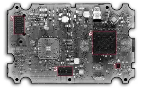
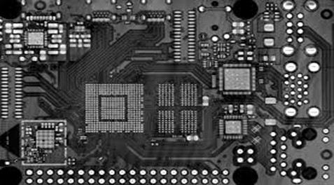
3D Imaging, X-rays penetrate printed circuit board materials at different rates based on density. FR-4 substrate permits X-rays through easily because it has low density. Copper traces block more X-rays because copper is dense metal. Lead-free solder blocks even more X-rays than copper. This different absorption generates contrast in X-ray images. Denser materials look darker in X-ray images because they block more radiation. Copper traces show up dark against the lighter FR-4 background. Solder joints seem very dark. Less dense materials like FR-4 substrate and air gaps appear lighter or nearly transparent. The result is that you see internal copper traces, via connections, and component solder joints without opening the circuit board.
Why Traditional Methods Fall Short
Visual PCB inspection only shows surface layers. You remain completely unsighted to internal structures in multilayer boards. Cameras and microscopes cannot penetrate the substrate to expose buried traces or internal vias. Destructive delayering removes layers sequentially using chemicals. You photograph each layer before dissolving it away. This destroys the original board permanently. You cannot verify your results against the original. Any mistakes in documentation become permanent. The process takes 2-4 weeks for complex boards.
Manual probing with multimeters traces connections one at a time. This shows extremely time-consuming on boards with thousands of connections. Limited accuracy arises from human error during repetitive work. You easily damage delicate traces with probe tips. For 8-layer and higher boards, manual methods take weeks while X-ray completes analysis in hours.
Applications Requiring X-Ray Analysis
- Multilayer PCB reverse engineering becomes practical with X-ray for printed circuit boards with 6 or more layers.
- Quality control distinguishes manufacturing defects before they reach customers.
- Counterfeit detection compares suspect boards versus authentic designs
- Failure analysis detects broken vias, solder joint cracks and delamination between layers.
Types of X-Ray Imaging for PCB Analysis
2D X-Ray Inspection (Basic Level)
Single-angle X-ray projection produces a 2D shadow image of your PCB. This works well for basic via inspection, solder joint quality checks, and component placement verification. You see if BGA balls connected properly or if vias formed completely.
Limitations contain trouble in recognizing overlapping features. Multiple layers project onto the same 2D image making interpretation challenging. You get no extent information about which layer contains specific features. Best use examples include simple inspection tasks, BGA solder joint inspection, and basic quality control where you need speedy pass/fail decisions.
3D Imaging and CT Scanning (Advanced)
Multiple X-ray images captured from different angles get reconstructed into a complete 3D Imaging model. You can digitally slice through the board at any depth to see any layer clearly. The complete 3D (Computed Tomography)reconstruction shows all traces, all vias including buried and blind types, and component internal structures.
Resolution ranges down to 1-5 microns, enough to see individual traces clearly. Process time runs 30 minutes to 3 hours depending on printed circuit board size and desired resolution. Equipment costs highly for industrial-grade CT systems. This investment makes sense for companies doing frequent reverse engineering or quality control work.
Laminography (Specialized)
Laminography is used specifically for flat objects like PCBs. This technique works better than traditional CT for thin boards. The system focuses on one specific layer while blurring others. This produces faster results than full 3D CT with better layer separation. You use laminography when analyzing specific internal layers without requiring complete 3D reconstruction of the entire board.
| Feature | 2D X-Ray | 3D CT Scan | Laminography |
| Resolution | 10-20 microns | 1-5 microns | 5-10 microns |
| Speed | Seconds | 30 min – 3 hrs | 15-45 min |
| Cost | $50K-$150K | $200K-$500K+ | $150K-$350K |
| Depth Info | No | Full 3D | Layer-specific |
| Best For | Quick QC, BGA | Complete RE | Specific layers |

How 3D Imaging X-Ray Tomography Works for PCB Reverse Engineering
Step 1: PCB Preparation and Mounting. You protect your PCB on a precision rotation stage. No special preparation is required. Scan the board as-is for completely non-destructive analysis. The fixture must not block X-rays or create artifacts in the final images.
Step 2: X-Ray Data Acquisition. The board rotates 360 degrees while the X-ray source and detector remain at rest. The system captures hundreds to thousands of 2D X-ray projections during rotation. Typical high-resolution scans use 1,000 to 2,000 images. Scan parameters containing voltage (50-150 kV), current, and exposure time get optimized for PCB materials to maximize contrast.
Step 3: 3D Reconstruction. Specialized software implements tomographic reconstruction algorithms to the X-ray projections. This creates a 3D voxel dataset, the three-dimensional equivalent of pixels. You obtain a complete digital model of the PCB’s internal structure. Processing time runs 15 minutes to 2 hours depending on board complexity and desired resolution.
Step 4: Analysis and Layer Extraction. Analysis software lets you slice through the board digitally at any depth. Extract individual layers as 2D images for detailed trace analysis. The system detects vias, buried vias, and blind vias automatically. 3D visualization shows all connections in proper spatial context.
Step 5: Schematic Generation. Convert the 3D data to layer-by-layer trace maps. Map all electrical connections between components. Generate complete schematic and netlist files from the internal structure data.
3D ImagingPCB X-Ray vs Traditional Delayering Methods
The comparison between PCB X-ray tomography and traditional delayering shows extraordinary differences:
| Factor | 3D X-Ray Tomography | Traditional Delayering |
| Board Preservation | Non-destructive, intact | Destroys original |
| Time Required | 4-8 hours total | 2-4 weeks manual |
| Accuracy | 95-99% (1-5µm) | 90-95% (human error) |
| Layer Count Limit | 20+ layers, no limit | Difficult beyond 10 |
| Cost per Board | $500-$2,000 service | $2,000-$8,000 labor |
| Repeatability | Perfect – can rescan | Impossible – destroyed |
| Via Analysis | Excellent – all types | Difficult for buried |
Applications for X-Ray PCB Imaging
Reverse engineering applications include multilayer board analysis for 6, 8, 10, and 12+ layer PCBs. HDI (High Density Interconnect) boards with micro vias need X-ray 3D imaging for complete understanding. Legacy equipment without documentation becomes maintainable. Competitive product analysis proceeds within legal bounds to understand design approaches.
Quality control and inspection protect BGA solder joint inspection where you cannot see connections visually. Via formation verification catches open vias and incomplete plating before boards reach production. Counterfeit component detection exposes inferior internal construction. Assembly defect identification finds problems early in manufacturing.
Failure analysis identifies cracks in solder joints, traces, or substrate material. Delamination identification between layers explains reliability failures. Thermal damage assessment shows overheating effects. Short circuit location in internal layers becomes straightforward instead of nearly impossible.
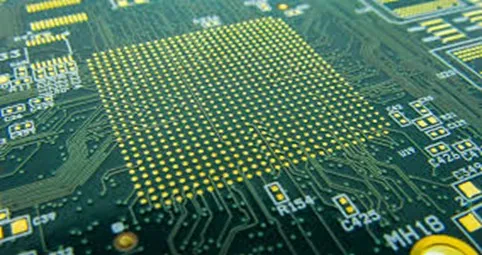
Limitations and Challenges of X-Ray PCB Imaging
Technical limitations include failure to see component internal die structures or firmware and software content. Resolution limits mean very fine features below 1 micron may not be visible. Material challenges occur when very thick copper planes block underlying features. Dense components can make shadows or streak artifacts in the final images.
Operational challenges include radiation safety requirements including shielded rooms, safety protocols, and licensing. Equipment cost represents high initial investment for in-house capability. Operator training needs specialized knowledge for optimal results. Data size challenges emerge as 3D CT generates gigabytes of data per scan requiring substantial storage and processing power.
Why Choose Wonderful PCB for X-Ray PCB Analysis
Wonderful PCB works fpr high-resolution 3D CT scanners with 1-5 micron resolution. We handle boards up to 400mm x 400mm with 20+ layers. Both 2D X-ray and 3D CT capabilities exist in-house with latest reconstruction software for optimal image quality. Our complete reverse engineering services merge X-ray imaging with expert analysis and schematic generation. We integrate optical inspection for surface verification and electrical testing to validate X-ray findings.
With years of PCB reverse engineering experience across thousands of multilayer boards, we guarantee 98%+ accuracy on delivered schematics. Our value-added services take you from X-ray analysis to full PCB reproduction including redesign, manufacturing, and assembly. Fast turnaround delivers results in 5-10 days for complete reverse engineering projects.
Frequently Asked Questions
Can X-ray imaging damage my PCB or its components?
No, X-ray imaging is completely non-destructive. The X-ray dose used for PCB inspection is very low and causes no damage to the board, components, or functionality. After scanning, your PCB works exactly as before.
What layer count requires X-ray vs optical inspection?
For 2-4 layer boards, optical inspection is usually sufficient. For 6+ layer boards, X-ray imaging is highly recommended to see internal layers. For 8+ layers, X-ray is practically essential for accurate reverse engineering.
How long does 3D X-ray tomography take?
Scanning takes 30 minutes to 3 hours depending on board size and resolution. 3D reconstruction adds 15 minutes to 2 hours. Total process from loading board to final analysis runs 4-8 hours. Complete results with expert analysis are delivered in 3-7 days.
What file formats do you provide after X-ray analysis?
We provide raw 3D volumetric data in DICOM format, layer-by-layer 2D images as TIFF or PNG files, 3D visualization files in STL format for viewing, extracted trace maps, and final schematics in your preferred CAD format including Eagle, Altium, and KiCad.
Is X-ray imaging worth the cost for my project?
For multilayer boards with 6 or more layers, yes. X-ray PCB imaging costs $1,000-$2,000 but saves weeks of manual delayering that costs $3,000-$8,000 in labor. You also preserve your original board for testing and verification. For simple 2–4-layer boards, optical methods are usually sufficient and more cost-effective.
Conclusion
3D X-ray tomography revolutionizes multilayer PCB reverse engineering. The technology brings non-destructive analysis completing in hours instead of weeks. You preserve your original board while achieving 95-99% accuracy with micron-level resolution. X-ray imaging proves essential for 6+ layer boards, HDI designs, quality control, and failure analysis applications. Cost-effectiveness comes from saving time and money versus traditional delayering methods. Technology continues advancing with equipment becoming more accessible and resolution improving. For multilayer PCB reverse engineering, X-ray tomography represents the modern standard approach.
Need X-ray analysis for your multilayer PCB? Wonderful PCB offers high-resolution 3D CT scanning with expert analysis. Get non-destructive reverse engineering with 98%+ accuracy. Contact us for a free consultation and quote.
Contact Us: Email: [email protected]
Phone: +86 0755-86229518
Visit: www.wonderfulpcb.com