You want the best PCB reverse engineering solution for you. The right choice depends on features that matter in engineering. When you compare services and tools, look at these things:
Schematic capture lets you draw and change circuit diagrams.
PCB layout tools help you put parts and find mistakes.
3D modeling shows how the pcb fits in a product.
Simulation and analysis test designs before you build them.
File import and export keep your work easy to use.
User interface saves time and helps you make fewer mistakes.
Community and support give help and resources.
Key Takeaways
Pick professional services if you want quick and correct results for hard PCBs. These experts help you and save your time.
Community and DIY choices are good for learning and saving money. You can use online forums and open-source tools to get better at this.
Pick software that matches your project. Tools like Altium Designer and KiCad help you with schematics and layouts.
Keep your data safe when doing reverse engineering. Use strong agreements and check your security often so no one steals from you.
Learn the legal rules about PCB reverse engineering. Respect intellectual property to stay out of trouble and be fair.
PCB Reverse Engineering Services Overview
Professional Service Providers
There are many companies that do pcb reverse engineering. These companies help you rebuild board data and update old designs. They also make new files for building boards. You get expert help and good results. Here are some top companies and what they do:
Company | Main Offerings |
|---|---|
UGPCB | Multilayer boards, HDI boards, flexible boards, special material PCBs, physical layer reverse analysis, component and code analysis, design optimization, BOM and schematic generation, prototype verification, mass production. |
A&P Material Supply | Single-layer boards, multi-layer boards, HDI designs, GERBER file creation, BOM documentation, design optimization. |
Datest | CAD file generation, electronic schematics, net list and part list creation, updating/modifying obsolete boards. |
Datest helps you make CAD files and board data from old pcb assemblies. This service lets you build boards without the original files. You can fix old designs and get all board data, like schematics and part lists.
Professional pcb reverse engineering services work fast. Simple boards may take only one or two days. Hard boards, like 8-layer ones, can take up to a week. Some jobs, like a 4-layer industrial board, cost about $850 and take five days. Better solutions can save you money and time. For example, you might pay $620 and wait three days for the same board. Big jobs often take three to eight weeks and cost between $3,000 and $25,000. You get good results and clear paperwork.
Tip: Professional companies use advanced tools and methods. You get correct results and help for making many boards.
Community and DIY Services
You can also use community and DIY ways for pcb reverse engineering. These choices are good if you want to learn or save money. Many hobbyists and small groups use online forums and open-source tools. You get help from other people and can solve problems together.
Online groups share guides and tips for reverse engineering.
Open-source tools help you get schematics and layouts.
DIY kits let you scan and measure pcb boards at home.
Forums give advice on fixing problems and best ways to work.
Community services are not always as fast or accurate as professional ones. You may need more time and work to get good results. You learn by doing and can get better at engineering. These choices are good for easy projects or if you want to know how a pcb works.
Service Type | Cost | Turnaround Time | Support Level |
|---|---|---|---|
Professional | Higher | Fast | Expert, reliable |
Community/DIY | Lower/Free | Variable | Peer, self-guided |
Pick professional services if you want high-quality results, quick work, and help with hard boards. Community and DIY services are best if you want to learn, try things, or work on small projects.
Top PCB Reverse Engineering Software
You need good software to help with pcb reverse engineering. The right software makes your work easier and more correct. It helps you rebuild boards, check for mistakes, and make new designs. There are many tools you can pick for your engineering needs. Some tools work well for simple boards. Others are better for hard projects.
Schematic Extraction Tools
Schematic extraction tools turn a real pcb into a digital diagram. You use these tools to find connections and parts. They help you make a clear map of the board. Many engineers like these programs because they save time. They also help you make fewer mistakes.
Cadence OrCAD lets you draw diagrams and lay out boards. It helps you manage BOMs and use smart routing. This makes your work faster.
Mentor Graphics PADS helps you draw diagrams and lay out boards. It checks your design rules so you avoid mistakes.
Zuken CR-8000 gives you tools for drawing diagrams and laying out boards. It has smart routing and advanced diagram features.
These tools have features that help you:
Automated tracing finds links between parts fast.
Part libraries help you choose the right parts.
Error checking warns you about problems early.
Design rule checks keep your design safe.
3D modeling shows how the board fits in things.
Simulation tests your design before you build it.
Easy interfaces help you learn and save time.
Tip: Use a schematic extraction tool to start rebuilding or fixing a board. You get a clear diagram and can move forward with confidence.
Layout and Imaging Software
Layout and imaging software help you make and check the board’s design. You use these tools to rebuild layouts and trace outlines. Some programs are good for drawing and tracing. Others have more engineering features.
KiCad lets you test your design for problems with SPICE. It is good for small projects and learning.
Inkscape changes pictures to vectors. You use it to trace outlines and make neat layouts.
Krita lets you draw and trace pcb images.
Ansys checks for heat, stress, and signal problems.
Altium Designer tests circuits and checks for mistakes.
OrCAD tests both analog and digital circuits.
Allegro works well for hard layouts, like in cars or planes.
Eagle is easy for quick layout jobs.
Cadence Allegro helps you see and design hard boards.
AutoTrace changes pictures to vectors fast.
GIMP lets you change images and use design libraries.
Mentor Graphics PADS gives you routing and 3D views.
Altium Circuit Studio helps with diagrams and auto-routing.
Here is a table to compare layout and imaging software:
Feature | Layout Software | Imaging Software |
|---|---|---|
Multi-layer PCB Design Support | Yes | Limited |
Signal Integrity Analysis | Advanced tools available | Basic analysis |
3D Visualization Capabilities | Comprehensive 3D preview | Minimal 3D support |
Integration with Hardware | Exports industry-standard files | Limited export options |
Output Quality | High-quality manufacturing outputs | Standard outputs |
Layout tools help with multi-layer boards, which are used for dense designs. Signal integrity checks make sure your board works fast. 3D views help you see how parts fit together. Many layout tools let you export files for making boards.
Note: Pick layout and imaging software that fits your project size. If you work on big boards, choose tools with strong features and good output.
You can use these tools to get better at engineering. Try different programs to see which one works best for your pcb reverse engineering.
Essential PCB Hardware Tools
Scanners and Imaging Devices
Scanners and imaging devices help you see inside a pcb. These tools let you look at each layer without breaking the board. High-resolution scanners show tiny parts and connections. X-ray machines and computerized tomography give clear pictures of the board. You use these images to rebuild the layout and find hidden problems.
Here is a table with important details for scanners and imaging devices:
Specification | Description |
|---|---|
Source power | Shows how deep X-rays can go |
Detector objective | Tells how clear and wide the view is |
Filtering | Controls X-ray strength and lets strong rays pass |
Distance of detector to sample | Closer means more counts |
Number of X-ray projections | Sets how much the board turns for each scan |
Exposure Time | Changes how long scanning takes and the cost |
You can use X-ray (2D) and computerized tomography (3D X-ray) to look inside the pcb. These ways do not hurt the board. Advanced CT scanning and laminography let you see all layers at once. You get correct maps of traces and parts.
Tip: Non-destructive imaging helps you study hard boards and find problems you cannot see with your eyes.
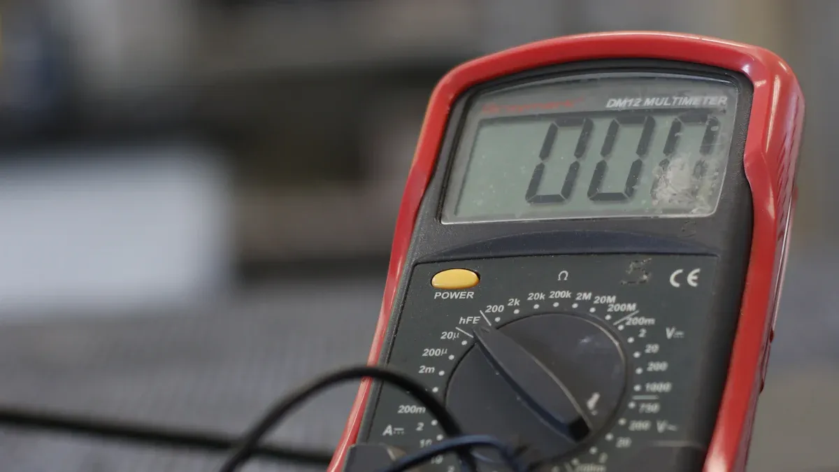
Measurement Equipment
Measurement equipment helps you test and check the pcb. You use these tools to measure voltage, current, and resistance. Multimeters give quick and correct results. Oscilloscopes show electrical signals. Logic analyzers help you study digital systems. SMD LCR meters measure small parts on the board. Power supplies let you control voltage and current safely.
Here is a table with common measurement equipment:
Equipment Type | Description |
|---|---|
X-ray Machines | Show hidden parts and shapes inside the pcb. |
X-ray Detectors | Catch X-rays and make clear digital pictures. |
X-ray Inspection Software | Study images and make them better. |
Multimeters | Measure voltage, current, resistance, and check if traces connect. |
Oscilloscopes | Show and study electrical signals. |
Logic Analyzers | Catch and study digital signals. |
Digital multimeters help you find good connections fast. SMD LCR meters give correct readings for small parts. Adjustable power supplies help you control voltage and keep things safe when you turn on the board. You need the right tools to get the best results in pcb reverse engineering.
PCB Reverse Engineering Workflow
Assessment and Preparation
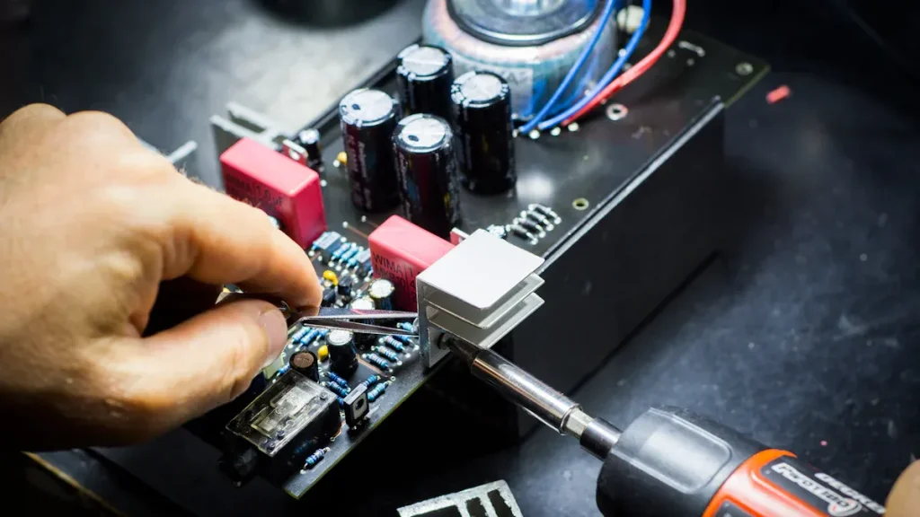
First, you look at the pcb very closely. You check its type and size. You count how many layers it has. You see if there are any special parts. You use microscopes and cameras to see small details. You plan which methods will work best for your board. If your pcb has many layers, you pick how to study it. Non-destructive ways keep the board safe. Destructive ways help with old or broken boards.
Imaging and Data Capture
You use scanners and cameras to take pictures of the pcb. High-resolution cameras show tiny parts. X-ray machines let you see inside the board. X-rays show hidden traces and parts. Automated tools can scan and save data fast. These steps help you get all the info you need.
Tip: Non-destructive imaging helps you study boards without breaking them.
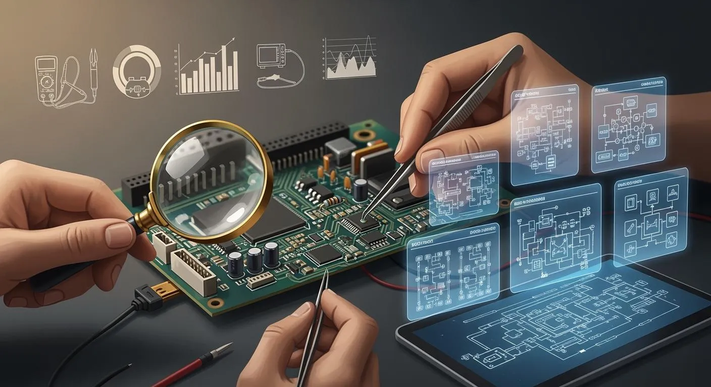
Data Processing and Analysis
You use software to look at the pictures and data. Programs like Altium Designer and KiCad help you make digital copies. You trace connections and rebuild the schematic. Automated methods save you lots of time. You can finish a big board in one or two weeks. You also check noise margins to keep signals strong.
Documentation and Output
You make a Bill of Materials with all the parts. You write down every step you take. You use software to make files and diagrams. Good records help you build new boards and fix problems. You keep these records for future projects.
Workflow Step | Main Tools Used | Special Techniques |
|---|---|---|
Assessment | Microscopes, cameras | Non-destructive, destructive |
Imaging/Data Capture | Scanners, X-ray machines | Automated scanning |
Data Processing | Altium Designer, KiCad | Automated tracing |
Documentation | BOM software, CAD tools | Schematic generation |
Note: Careful records and good methods help your pcb reverse engineering project work well.
Challenges and Best Practices
Multi-Layer and Complex Boards
Working with multi-layer and complex boards can be hard. These boards often do not have any instructions. It can be tough to figure out how the pcb works. Many layers make it tricky to follow connections. You must be careful not to break the board. Sometimes, part numbers are faded and hard to read. Custom parts can make things even harder. You might need to find new parts if old ones are gone. Time and money can also make your job stressful. You need to work quickly but still be correct.
No instructions make learning about the board hard.
Many layers make following connections risky.
Faded numbers and custom parts are hard to identify.
Old parts may need new designs or replacements.
Time and money worries can slow you down.
Tip: Take good pictures and write notes at every step. This helps you remember what you did and avoid mistakes.
Obsolete or Damaged PCBs
You will often work with boards that are old or broken. Getting data from these pcbs is not easy. Some studies show you can use gravity and electrostatic separation to get metals from old boards. Electrostatic separation works well for tiny pieces and gives lots of metal. Some engineers use chemicals like hydrometallurgy or bio-leaching. These ways can use a lot of energy and may cause pollution. Scientists keep looking for safer and better ways to get materials. You should pick methods that help the environment and give good results.
Data Security and Confidentiality
You need to keep your designs safe during pcb reverse engineering. If you do not protect your data, someone might copy your work. They could sell your design or use it for their own products. This can make you lose money and hurt your reputation. Other companies might use your ideas and take your place. You could also have legal trouble if someone breaks your rights.
Someone might copy and sell your design.
Engineers could find and use your secrets.
Workers might steal files and share them.
Weak safety can cause lawsuits and lost money.
Hackers might find weak spots and attack you.
You can use smart steps to keep your data safe. The table below shows some important things to do:
Best Practice | Description |
|---|---|
Ownership and IP Rights | Make clear rules for who owns the design and IP. |
Confidentiality Obligations | Use strong rules and agreements to keep secrets. |
Prohibitions on Reverse Engineering | Do not allow others to use or copy your work without permission. |
Indemnification and Liability | Add rules to protect yourself from legal trouble. |
Dispute Resolution | Plan how to solve problems with contracts. |
Note: Use strong NDAs, good encryption, and limit who can see files. Check your security often to find and fix problems early.
Legal and Ethical Issues in PCB Reverse Engineering
Intellectual Property
It is important to know intellectual property rules first. These rules protect designs and ideas from being stolen. If you copy a patented design without asking, you can get in trouble. You need to respect these rights to avoid lawsuits and be fair. Many places, like the Americas and Asia-Pacific, use strong data rules to stop theft.
Copying patented designs without permission can cause big problems.
Use reverse engineering for learning, fixing, or making new things, not stealing.
Board makers use tricks to keep their designs safe. They hide part numbers, change the size of passive parts, and use special security to make copying hard.
You will find different laws that protect PCB designs. Here is a table to help you learn:
Type of Law | Description |
|---|---|
Copyright | Protects original works like PCB designs. You need to register for full legal protection. |
Trademark | Protects brand names, not the PCB design or schematic. |
Patent | Protects inventions and designs for 20 years. Others cannot use the patented design. |
Trade Secret | Protects secret knowledge. You need agreements to keep your secrets safe. |
Note: Always check the laws in your country before you start. Following the rules helps you stay out of trouble.
Compliance and Regulations
You must follow rules when you reverse engineer PCBs. These rules help keep your work safe and legal. Some rules control how you share and move boards and data.
Compliance Area | Description |
|---|---|
Export/Import of Assembled Boards | Rules for moving PCBs and parts between countries. |
Sharing Manufacturing Data | Limits on sharing files like Gerber data with people outside the U.S. |
Sharing Design Data | Restrictions on sharing design plans with non-U.S. persons. |
Different industries have special standards. For example, cars need rules to stop electronic interference. Environmental rules like RoHS keep electronics safe by banning dangerous materials. You also need to pick materials that can handle heat, water, and stress.
EMC stops electronics from messing with each other.
RoHS keeps electronics safe and green by banning bad substances.
Good materials help your board last longer and follow safety rules.
Tip: Always check industry standards and local laws before you start your project.
Choosing the Right PCB Solution
For Professionals
You need a solution you can trust for pcb design. Engineers often work with hard boards and strict rules. It is important to keep good records for every step. This helps you see what changed and share with your team. You should know each board’s details. Check how many layers it has. Look at the materials and where parts go. Think about problems like electromagnetic interference. Signal integrity and heat can change how your board works. These things matter in real life.
You can use special software and hardware for better results. Many engineers pick tools that trace parts by themselves. They also check for mistakes and show 3D models. Fast service and expert help are good to have. The right choice saves time and helps you make fewer errors.
Tip: Make sure the service follows rules and keeps your data safe.
Criteria | Why It Matters |
|---|---|
Documentation | Tracks progress and changes |
Guides tool selection | |
EMI/SI/Thermal Concerns | Ensures reliable operation |
For Hobbyists
You might want to learn about electronics or fix boards at home. Hobbyists like easy and cheap solutions. You can use free software and DIY kits. These help you scan and rebuild simple boards.
Join online groups and forums to get help. People share guides and tips. You can ask questions and get answers. Many hobbyists use free programs to draw diagrams. You do not need expensive tools for small jobs.
Note: Try different tools to see what works best. Practice makes you better and helps you learn how boards work.
Solution Type | Cost | Support Level | Best For |
|---|---|---|---|
Open-source tools | Free | Community help | Learning, repairs |
DIY kits | Low | Self-guided | Small projects |
Online forums | Free | Peer support | Troubleshooting |
You can have fun and learn new things. Start with easy boards. Move to harder ones as you get better.
You have many choices for PCB reverse engineering. Professional services give you speed and accuracy. Community tools help you learn and save money. Software and hardware tools make your work easier.
Choose a solution that fits your project size and skill level.
Look for strong support and clear documentation.
Protect your data and follow legal rules.
Tip: Match your tools and services to your needs. This helps you get the best results.
FAQ
What is PCB reverse engineering?
PCB reverse engineering means making a copy of a board’s design. You do this when you do not have the original files. This helps you fix, change, or learn from old electronics.
Can you reverse engineer a multi-layer PCB at home?
You can work on simple boards at home. Multi-layer boards are harder to do yourself. You need special tools like X-ray scanners to see inside. These tools let you look at the board without taking it apart.
Is PCB reverse engineering legal?
You should check your local laws before starting. In many places, it is okay for learning or fixing things. If you copy to sell or break patents, you can get in trouble.
What software do you need for PCB reverse engineering?
You need programs for drawing diagrams and layouts. Some good ones are KiCad, Altium Designer, and Inkscape. These help you make schematics and rebuild the board’s layout.