When you work on printed circuit board projects, pcb copy software like Altium Designer, KiCad, and Eagle helps you a lot with pcb reverse engineering. You often need both computer tools and real tools to find out how a pcb works and fix problems. PCB reverse engineering lets engineers repair, change, or make a pcb better when the original papers are gone. By using the right pcb copy software and tools, you can finish your work faster and learn more about how the board is built.
Key Takeaways
Pick the right PCB copy software like Altium Designer, KiCad, or Eagle. This helps you work faster and makes your designs better.
Use different software tools for drawing, 3D modeling, and testing. This helps you make PCB layouts that are correct and work well.
Use hardware tools like scanners, multimeters, and soldering irons. These help you get clear pictures and measure your PCB the right way.
Follow easy steps: scan the board, work on the images, rebuild the schematic and layout, and test your design with care.
Always check the law before copying PCBs. Plan your work so you do not make mistakes and can finish your projects quicker.
PCB Copy Software Overview
Leading PCB Copy Software
If you want to do pcb reverse engineering, you need the right pcb copy software. There are many choices, and each one helps with different steps. Here are some of the best ones you can try:
Altium Designer: This pcb design software is good for big projects. It has strong layout and schematic tools. Many engineers pick Altium because it has lots of features and works with hard pcb boards.
KiCad: This open-source software lets you make and change pcb layouts for free. It has many tools for both easy and hard boards. KiCad is great for students, hobbyists, and some engineers.
Eagle: Autodesk Eagle helps you with pcb layout and schematic capture. You can use it for small or big designs. Many people like Eagle because it is simple to use.
OrCAD: OrCAD has strong tools for schematic capture and pcb layout. Many companies use OrCAD for engineering and making things because it works with big, hard boards.
Allegro: Cadence Allegro is a high-level pcb copy software. You can use it for big jobs in car and airplane industries. Allegro helps with hard layouts and making boards.
DesignSpark PCB: This free software helps you design and copy pcb layouts. You can use it for fast projects or to learn about pcb design.
QuickPcb2005: You can use this tool for easy pcb layout and editing. It is good for simple reverse engineering jobs.
Autodesk Fusion 360: Fusion 360 gives you 3D modeling and pcb design tools. You can see your board in 3D and check if it fits in your product.
FreeCAD: FreeCAD lets you make 3D models of pcb boards. You can use it to check the fit and design before making your board.
SolidWorks: SolidWorks helps you with 3D modeling and engineering. You can use it to design cases and check pcb layout in real products.
Ansys: Ansys gives you simulation tools. You can test your pcb for heat, stress, and other problems before building it.
Krita and Inkscape: These image editing tools help you trace pcb layouts from scanned pictures. You can use them to clean up pictures and get them ready for layout work.
Tip: You can use more than one software tool to get better results. Some are best for layout, and others help with 3D modeling or testing.
Key Features to Consider
When you choose pcb copy software, look for features that fit your project. Here are some important things to check:
Schematic Capture: You need to draw and change circuit diagrams. Good software makes this easy.
PCB Layout Tools: Look for strong layout tools. You want to place parts, draw lines, and check for mistakes.
3D Modeling: Some projects need 3D views. This helps you see if your pcb fits in a case or product.
Simulation and Analysis: You can test your design before making it. Simulation tools help you find problems early.
File Import and Export: You need to move files between software tools. Good pcb copy software works with many file types.
User Interface: Easy software saves you time. Look for clear menus and helpful guides.
Community and Support: Some software has big user groups. You can find help, guides, and answers to your questions.
You will see differences between professional and hobbyist tools. Professional pcb copy software like Altium Designer, OrCAD, and Allegro has more features for big and hard boards. These tools cost more and need more training. Hobbyist tools like KiCad, DesignSpark, and QuickPcb2005 are free or cheap. They are good for small projects and learning. You can start with hobbyist tools and use professional software as you get better at engineering.
Note: Always check if the software works with the way you want to make your board. Some tools make it easy to create files for factories, but others need extra steps.
You can use pcb copy software to finish your reverse engineering work faster. The right software tools help you make good layouts, test your design, and get your board ready to build. You save time and make fewer mistakes when you pick the best tools for your needs.
PCB Reverse Engineering Basics
What is PCB Reverse Engineering
You may wonder what pcb reverse engineering means. When you do pcb reverse engineering, you study a printed circuit board to learn how it works. You look at the board, find the parts, and trace the circuit paths. This process helps you understand the design and function of the pcb. Sometimes, you need to do this when you do not have the original design files or documents.
You can use tools to help you see each layer of the pcb. You might scan the board or take clear photos. You then use these images to map out the circuit. Many engineers use pcb reverse engineering to fix broken boards, improve old designs, or check how a product was made. This work helps you learn more about engineering and circuit design.
Tip: If you want to repair or upgrade a device, reverse engineering pcb board can show you the steps the original designer took.
Why Use PCB Copy Software
You need the right software to make pcb reverse engineering easier and faster. PCB copy software lets you draw the circuit, rebuild the layout, and test your ideas. With these tools, you can turn your images and notes into a working design. You can also check if your new design matches the old pcb.
Here are some reasons to use pcb copy software:
You can create a new schematic from an old pcb.
You can test your design before you start manufacturing.
You can save time by using software tools instead of drawing by hand.
You can share your work with other engineers.
Many companies use pcb reverse engineering to keep products working when parts are no longer made. You can also use these skills to learn more about circuit design and manufacturing. When you use software, you make the reverse engineering pcb board process more accurate and less stressful.
Essential Hardware Tools for PCB
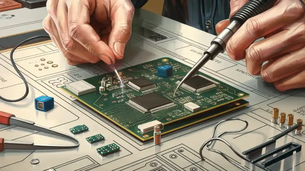
When you start pcb reverse engineering, you need special hardware tools. These tools help you look at the board and measure things. The right equipment helps you work faster and make fewer mistakes.
Scanners and Cameras
You need good pictures of your pcb. High-resolution scanners show small details on the board. Flatbed scanners work for boards with one or two layers. If your board has many layers, use a digital camera with a macro lens. You can take close-up photos from different sides. Clear pictures help you see the paths and find all the parts.
Tip: Put your pcb on a clean, flat table before you scan or take pictures. This gives you better and sharper images.
Test and Measurement Tools
You have to check the parts and lines on your pcb. A multimeter lets you measure voltage, resistance, and if lines connect. An oscilloscope shows how signals move on the board. Logic analyzers help you test digital signals. These tools help you find broken lines or bad parts. LCR meters let you measure inductance, capacitance, and resistance.
Multimeter: Measures simple electrical values.
Oscilloscope: Shows how signals look.
Logic Analyzer: Checks digital circuits.
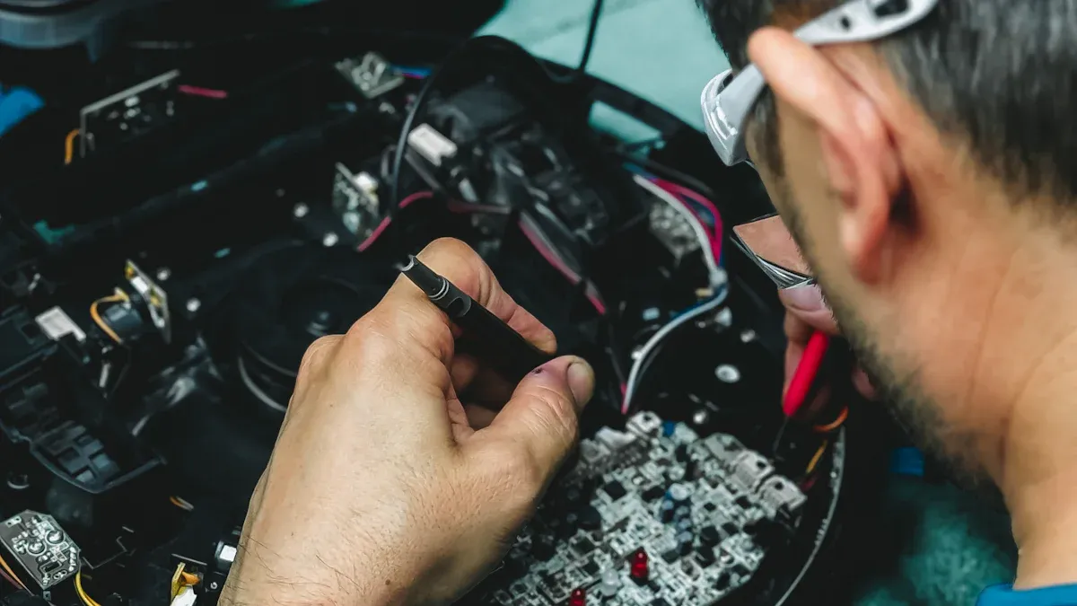
Board Preparation Tools
You may need to get your pcb ready before you scan or test it. Soldering irons help you take off or put on parts. Depaneling tools let you cut the board if you need to. Tweezers and small brushes help you clean off dust and dirt. Magnifying glasses help you see tiny things. These hardware tools make your work easier and safer.
Note: Always wear safety glasses when you cut or solder a pcb.
You can finish your reverse engineering project faster with the right hardware tools. Good planning and careful measuring help you get better results.
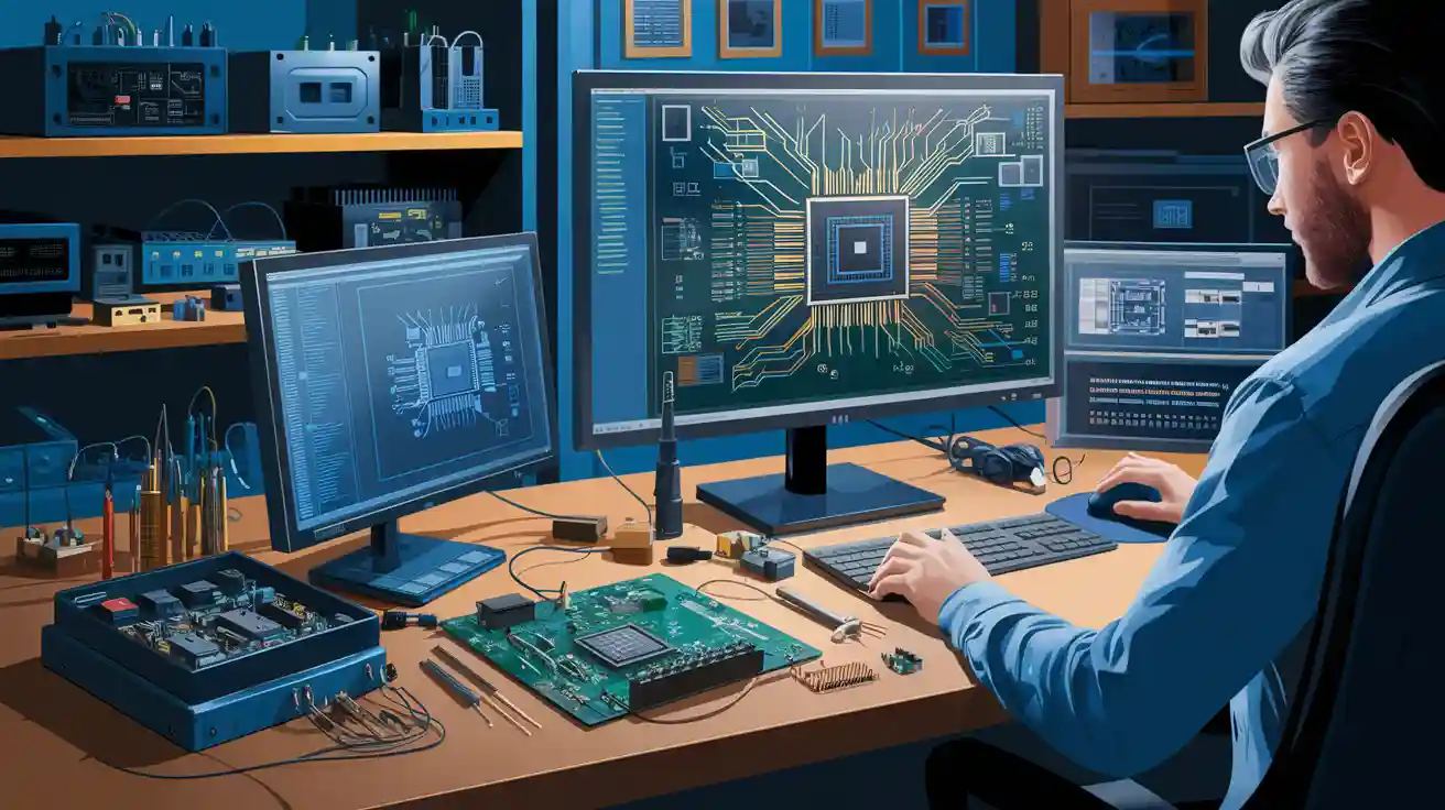
Software Tools for Reverse Engineering
When you start reverse engineering a pcb, you need good software tools. These tools help you draw the circuit, make the pcb layout, and test your design. You can use different software for each step. Some tools are best for drawing circuits. Others help you see your board in 3D or run tests.
Schematic Capture Tools
You must draw the circuit before making the pcb. Schematic capture tools help you make clear circuit diagrams. OrCAD, Altium Designer, and KiCad are good choices. OrCAD is strong for big projects. Altium Designer links your diagram to the pcb layout. KiCad is free and easy for students and engineers.
OrCAD: Good for big and hard circuit diagrams.
Altium Designer: Connects your diagram to the pcb layout.
KiCad: Free and open-source, good for learning and small jobs.
These tools help you keep each part of the circuit organized. You can name parts, draw lines, and check for mistakes. When your diagram is done, you can move to the next step.
Tip: Always check your circuit diagram before starting the pcb layout. This helps you stop mistakes early.
Layout and 3D Modeling Tools
After the diagram, you need to make the pcb layout. Layout tools help you put parts in place and draw lines. Altium Designer, Allegro, and Eagle are popular for this job. Altium Designer has strong features for big boards. Allegro is good for cars and planes. Eagle is simple and good for small boards.
Altium Designer: Strong pcb layout and 3D view.
Allegro: Handles hard layouts for industry.
Eagle: Easy for quick pcb layout jobs.
3D modeling tools let you see your board in real life. SolidWorks, FreeCAD, and Fusion 360 help you build a 3D model of your pcb. You can check if your board fits in a case. Fusion 360 lets you do layout and 3D modeling together. FreeCAD is open-source and good for simple 3D jobs.
Note: 3D modeling helps you find problems before building your pcb. You can save time and money by checking the fit early.
Some engineers use special tools to speed up reverse engineering. These tools can scan your board and help you make the layout faster. You can also use image editing software like Krita and Inkscape. These programs let you trace pcb layouts from pictures. You can clean up images, draw over lines, and get files ready for layout.
Krita: Edit and trace pcb images with drawing tools.
Inkscape: Trace outlines for clean pcb layouts.
Simulation and Analysis Tools
Before you build your pcb, you should test your design. Simulation and analysis tools let you see how your circuit works. Ansys is a strong tool for testing your pcb. You can see how heat, stress, and signals affect your board. Altium Designer and OrCAD also have simulation features.
Ansys: Runs tests for heat, stress, and signals.
Altium Designer: Simulates circuits and checks for mistakes.
OrCAD: Tests both analog and digital circuits.
Simulation tools help you find problems before making the board. You can change your design and test it again. This step saves time and helps you make a better pcb.
Tip: Use simulation early in your work. You can catch mistakes before they cost you.
You can use many software tools for reverse engineering. Each tool does a special job. Schematic capture tools help you draw the circuit. Layout and 3D modeling tools help you build and check the pcb layout. Simulation and analysis tools test your design before building. Special reverse engineering tools and image editing software make the job faster and more correct. When you use the right software, you finish your project with fewer mistakes and better results.
Reverse Engineering PCB Board Workflow
Board Scanning and Imaging
You begin by taking clear pictures of the pcb. Use a scanner or camera for pcb scanning. Lay the pcb flat on the table. Make sure the light is bright and even. Take photos of both sides of the board. If your pcb has many layers, you might need to remove some parts. This helps you see hidden lines and traces. Good pictures help you rebuild the pcb layout.
Tip: Wipe the pcb before you scan it. Dirt can cover up important lines.
Image Processing and Layer Alignment
After taking pictures, you need to fix the images. Use image editing software to make them brighter and clearer. This helps you see the circuit lines better. Line up the images of each layer so they match. You want the top, bottom, and inside layers to fit together. Getting the layers right is very important for reverse engineering pcb board. Every line and pad should be in the right place for the next steps.
Keep each pcb image on its own layer in your software.
Zoom in to spot tiny details.
Schematic and Layout Reconstruction
Next, you work on the schematic and pcb layout reconstruction. Follow each line from the pictures. Draw the schematic diagram with your software. Put every part where it belongs. Then use pcb layout tools to rebuild the board. This is the main part of reverse engineering pcb board. Check every connection to make sure it matches the old pcb.
Check each line twice to avoid mistakes.
Use your pictures to help with pcb layout reconstruction.
Verification and Testing
The last step is to test your pcb layout reconstruction. Look at your new layout and compare it to the old board. Use test tools to look for mistakes. Make sure every part works the right way. This step makes sure your reverse engineering pcb board project is correct. If you find a problem, fix it and test again.
Note: Careful testing helps you avoid problems later and saves time.
Challenges and Best Practices
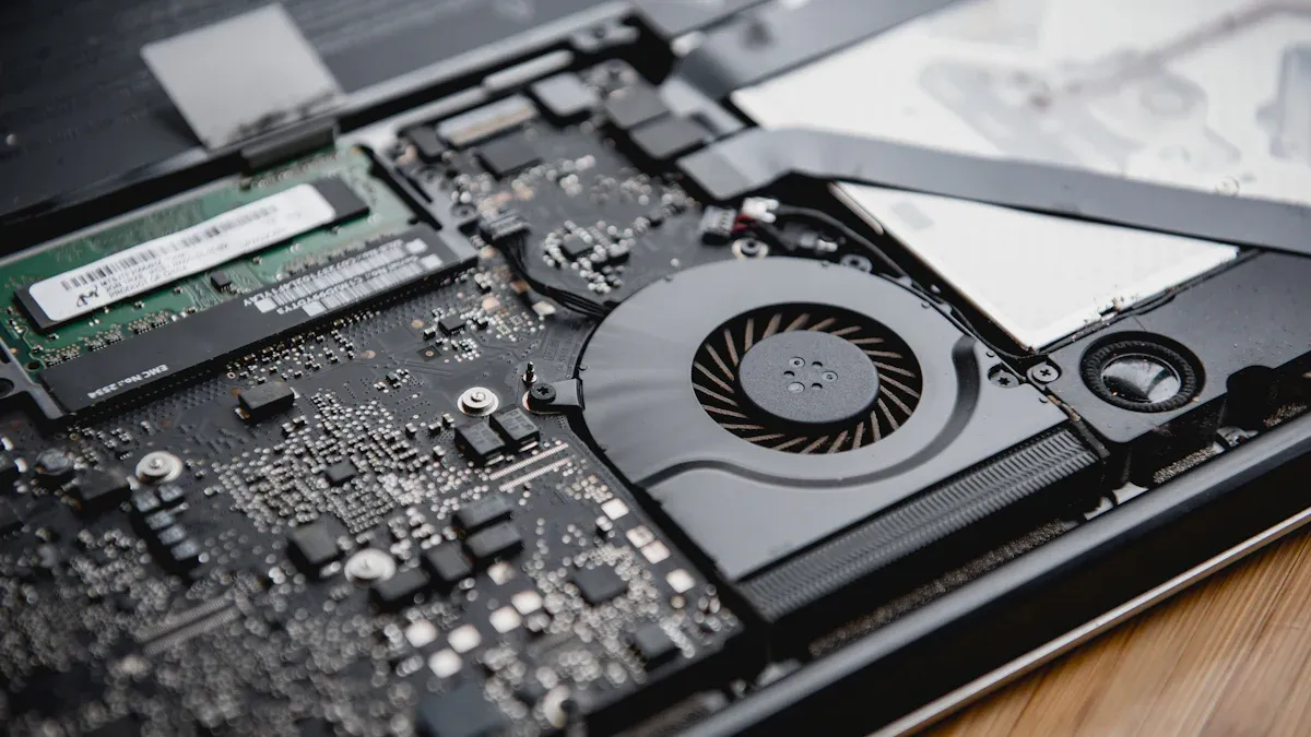
Multi-Layer Board Issues
Working with multi-layer pcb reverse engineering can be hard. These boards have many layers stacked on top of each other. Some layers hide traces and parts you need to see. You need special tools to look inside the board. High-resolution scanners and x-ray machines help you see each layer. You must take clear pictures and keep them in the right order. If you miss a layer, your design might not work right. Multi-layer pcb reverse engineering takes time and careful planning.
Data Accuracy and Error Prevention
Getting the data right is very important in pcb reverse engineering. You have to check every trace and part on the board. If you make mistakes, the pcb might not work after it is made. Use software tools to compare your design to the real board. Check your work at every step. Write notes and use documents and guides. These help you find mistakes early. Many engineers use netlist extraction and cross-checking to stop errors.
Tip: Save your work often. Back up your files so you do not lose them.
Legal and Ethical Considerations
You must follow the law when you do pcb reverse engineering. Some boards have patents or copyrights. You cannot copy them to sell or make money unless you have permission. Always check if you need a license first. Many companies offer pcb reverse engineering services that follow the law. Respect the work of other engineers and designers.
Workflow Optimization
You can finish your project faster if you plan your work well. Use the best software tools for each step. Make a plan before you start. Write a checklist for scanning, tracing, and design. Share your files with your team. Use reverse engineering techniques to make hard jobs easier. Good workflow helps you save time and stop mistakes in manufacturing.
Best Practice | Benefit |
|---|---|
Use clear images | Fewer errors in design |
Double-check connections | Better pcb performance |
Follow legal guidelines | Safe and ethical engineering |
Plan each step | Faster project completion |
Picking the best pcb copy software and hardware tools helps you do well in reverse engineering. You can use this simple checklist to help with your next pcb project:
Tool Type | Top Choices |
|---|---|
PCB Software | Altium, KiCad, Eagle |
Hardware Tools | Scanner, multimeter, iron |
Keep learning about new pcb tools and always use good engineering habits. Look for more resources to get better at your skills and learn more.
FAQ
What is the best PCB copy software for beginners?
You can start with KiCad or DesignSpark PCB. These tools are free and easy to use. You will find many guides and videos online. Both help you learn PCB design and reverse engineering step by step.
Can you reverse engineer a multi-layer PCB at home?
You can reverse engineer simple multi-layer PCBs at home. Use a scanner and camera for each layer. For complex boards, you may need special tools like X-ray machines. Always work carefully and keep your images organized.
Do you need both hardware and software tools for PCB reverse engineering?
Yes, you need both. Hardware tools help you see and measure the board. Software tools let you draw, test, and rebuild the design. Using both gives you better results and helps you avoid mistakes.
Is it legal to copy any PCB you find?
No, you cannot copy every PCB. Some boards have patents or copyrights. Always check the law before you start. You should only reverse engineer for learning, repairs, or with permission.
How do you check if your copied PCB design works?
You can use simulation tools like Ansys or Altium Designer. These tools let you test your design before you build it. You can also compare your layout to the original board and use a multimeter to check connections.