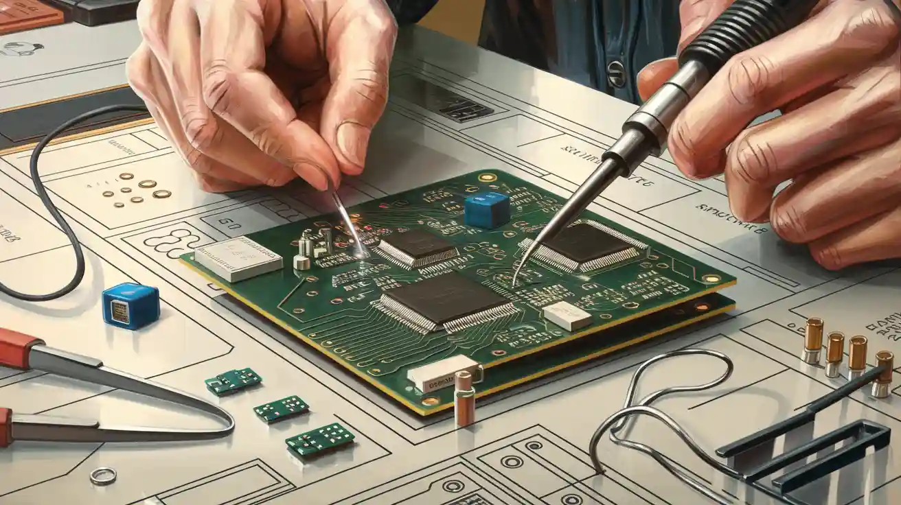
You can make a diy pcb right at home, even if you have never tried before. Many beginners use several different methods to create their own circuit boards. Here are some popular ways you might try:
Draw your circuit by hand on copper boards.
Use free PCB design software like KiCad.
Send your design to a service that makes the board for you.
Try rapid prototyping with simple tools.
You do not need fancy tools for every diy project. Sometimes, items from your kitchen or desk will do the trick. Give it a shot and see how creative you can get!
Materials and Tools
Basic Materials
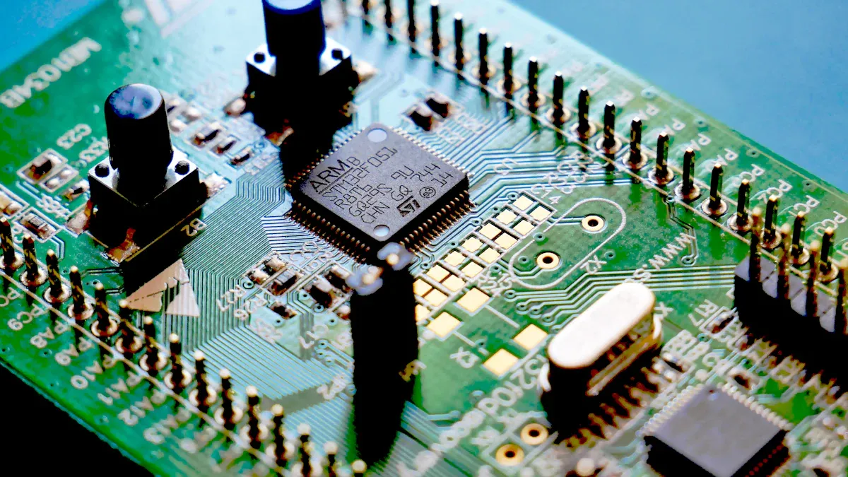
You need a few simple things to start making your own pcb at home. The most important item is a copper-clad board. This is a thin piece of board covered with a layer of copper. You will also want etching supplies. Many people use ferric chloride, but you can try safer household items like vinegar and hydrogen peroxide. These work well for small projects and are much less dangerous than industrial chemicals. They might take a bit longer, but they make the process safer and more beginner-friendly.
If you want to skip etching, you can use a perf board or veroboard. These boards have holes and copper tracks already in place. You just place your components and connect them with solder. This is a great way to build simple circuits without any chemicals.
Tip: If you want to design your circuit before building, try free software like KiCad. It helps you plan your pcb layout and avoid mistakes.
Essential Tools
You do not need a fancy workshop to get started. Here are some tools that make the job easier:
Soldering iron and solder wire
Multimeter with multiple probes
USB to serial bridge
Programmer
Basic oscilloscope
Current limiting DC power supply
A soldering iron lets you attach parts to your board. A multimeter helps you check your connections. The other tools help you test and program your circuit, but you can start with just the basics.
Optional Items
Some items are not required, but they can make your project smoother:
Safety glasses and gloves
Small drill or hand drill for making holes
Tweezers for tiny parts
Fine-tip marker for drawing circuit lines by hand
Old toothbrush for cleaning the board
You can find many of these items around your house or in a basic tool kit. With these materials and tools, you are ready to start your first pcb project!
DIY PCB Steps
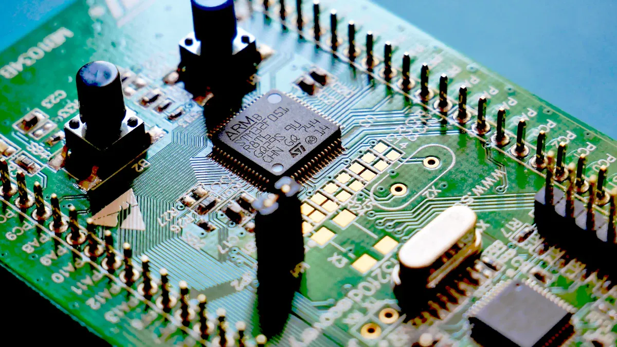
Making your own diy pcb at home feels exciting. You get to see your ideas come to life. Let’s walk through each step together, from design to soldering.
Design
You can start your diy pcb project with a pencil or with software. If you like drawing, grab a fine-tip marker and sketch your circuit right on the copper board. Keep your lines neat and clear. For more complex circuits, digital tools help a lot.
KiCad is a great choice for beginners. Here’s how you design a pcb using KiCad:
Open KiCad and create a new project. You get two files: one for the schematic and one for the pcb.
Add your components using the ‘Place Symbol’ tool. Connect them with the ‘Place Wire’ tool.
Run the Electrical Rules Checker to spot any mistakes.
Assign footprints to your parts so you know how they’ll look on the board.
Make a netlist and import it into the pcb editor.
Draw the shape of your board and add mounting holes.
Arrange your components on the layout.
Add graphics or text if you want.
Create a ground plane to help reduce noise.
Export your design as Gerber files for manufacturing.
Tip: If your design is large, mirror the image before printing. This helps you line up everything perfectly when you transfer it later.
Printing your pcb layout is easy. You need white A4 paper and glossy magazine paper. Here’s a simple way to do it:
Print your pcb design on regular paper.
Place glossy magazine paper on top and tape it down.
Cut the glossy paper a bit bigger than your layout.
Put your copper board on the glossy paper, copper side down.
Fold the paper around the board and tape it.
Put the wrapped board in a plastic container.
Pour nail polish remover over it.
Rub gently with your fingers to transfer the toner.
Let the paper dry, then peel it off.
This method works well for diy pcb projects. You get sharp lines and clear traces.
Prepare Board
Before you start the diy pcb manufacturing process, you need to get your copper-clad board ready. Clean the copper surface with an old toothbrush and some dish soap. This removes oil and dirt. Dry the board with a paper towel.
Safety matters. Here’s a table with some precautions:
Safety Precaution Type | Description |
|---|---|
Electric Safety Procedures | Use anti-static wristbands, check for exposed wires, and keep equipment grounded. |
Personal Protective Clothing (PPC) | Wear gloves, lab coats, face shields, and anti-static clothing. |
Waste Management and Environmental Safety | Shred scrap pcb, follow disposal rules, and use safer products when possible. |
Fire and Explosion Prevention | Store chemicals in fireproof containers and keep a fire extinguisher nearby. |
Worker Training and Awareness | Learn about hazardous materials and practice safety drills. |
Regulatory Compliance | Follow local safety and environmental rules. |
Transfer
Transferring your design to the board is a key step. The toner transfer method works best for diy pcb projects. You use the printed glossy paper and heat to move the toner onto the copper. This gives you sharp, reliable traces. Many hobbyists like this method because it’s quick and gives results close to professional printed circuit boards.
Note: Experiment with different printers and papers. You might find a combo that works best for your diy pcb.
Etch
Now you need to remove the extra copper. You can use ferric chloride, but kitchen supplies work too. Mix vinegar and hydrogen peroxide in a plastic container. Drop your board in and watch the copper disappear from the blank areas. This step takes patience. Check your board every few minutes.
Safety tip: Wear gloves and work in a well-ventilated area. Dispose of chemicals safely.
Drill
After etching, you need to make holes for your components. Use a small drill or hand drill. Here’s a quick guide for hole sizes:
Component Type | Recommended Hole Size (mm) |
|---|---|
Terminal blocks and trimmers | 1.2 to 1.5 |
ICs and resistors | 0.8 |
Larger connectors | 1.2 to 1.5 |
Go slow and steady. Clean out the holes with a toothpick if needed.
Solder
Soldering brings your diy pcb to life. Start with the smallest parts first. Place them on the board and heat both the lead and the pad with your soldering iron. Touch the solder to the joint and let it flow. You want a shiny, smooth connection. If you make a mistake, use solder wick to remove extra solder.
Here’s a simple soldering checklist:
Gather your soldering iron, solder wire, and solder wick.
Place small components first, then move to bigger ones.
Heat the joint and add a little solder.
Check for cold joints and fix them if needed.
Tip: Practice on scrap boards before working on your final diy pcb. You’ll get better with each try.
You’ve now finished all the steps for making your own diy pcb. Each part of the process helps you learn more about electronics and pcb design. Try different methods and see what works best for you!
Best DIY PCB Method
Choosing the best diy pcb method depends on what you want to build and how much time you have. You might want high precision, quick results, or just a simple way to get started. Let’s look at three popular methods and see which one fits your needs.
CNC Mill
If you want sharp lines and perfect accuracy, CNC milling stands out. You use a computer-controlled machine to carve out your circuit paths from a copper board. This method gives you clean edges and tight tolerances. You can make complex shapes and detailed designs.
Here’s a quick comparison:
Aspect | CNC Milling | Other Methods (e.g., Chemical Etching) |
|---|---|---|
Precision | High precision and accuracy | Generally lower precision |
Cost | Higher due to labor and tooling | Lower, simpler methods |
Complexity | Suitable for complex geometries | Limited to simpler designs |
CNC milling can cost between $150 to $250 for labor alone, depending on how tricky your design is.
Simpler methods like chemical etching usually cost less.
You get top-notch results, but you pay more and need special equipment. If you want to make a professional-looking pcb at home, CNC milling is a solid choice. For most beginners, though, it feels a bit too advanced.
UV Resin
UV resin is a cool way to make circuit boards quickly. You pour the resin onto your board, shine a UV light, and watch your design appear. This method works great for small projects and prototypes. You don’t need to mess with chemicals or wait for long etching times.
Here’s a table showing the pros and cons:
Advantages | Disadvantages |
|---|---|
Efficient and precise prototyping | Requires a learning curve for application |
Rapid iteration of designs and concepts | Can be messy and requires proper handling |
Democratizes high-resolution PCB prototyping | Not suitable for large-scale projects |
No need for traditional etching methods | UV light exposure can be harmful |
Cost-effective for small-scale developers | Sometimes dries sticky and can become patchy |
Allows for creativity in design | Yellows or becomes cloudy with harsh light |
You don’t need to mix anything—just pour and go.
Thin layers dry in two or three minutes.
Perfect for quick prototypes.
But you need a UV lamp, which adds to your costs. Sometimes the resin dries sticky or patchy. UV light can be harmful, so you need to be careful. This method works best for small, creative projects, not for big boards.
Perf Board
Perf board is the easiest way to start building circuits. You get a board with holes and copper pads already in place. You just push your parts through the holes and solder them down. You don’t need chemicals, printers, or fancy machines.
Perf board gives you a reliable and flexible base for your circuit.
You can test and change your design as you go.
It’s sturdy and perfect for experimenting.
If you’re new to electronics, perf board is the best diy pcb method to try first. You can build simple circuits and learn how everything works. Many guitar pedal fans use perf board for custom effects. You can even check out PedalPCB.com for ready-to-build pedal projects.
Tip: Start with perf board if you want to learn fast and avoid mistakes. You’ll get hands-on experience and see results right away.
Each method has its own strengths. CNC milling gives you precision, UV resin lets you prototype quickly, and perf board makes learning easy. Try them out and see which one feels right for you.
Mistakes to Avoid
When you start your diy pcb project, you might run into a few common mistakes. Knowing what to watch out for helps you get better results and saves you time.
Design Issues
You want your pcb to work well, so pay attention to your layout. Many beginners think that following the minimum clearance is enough, but this can cause problems with noise and make manufacturing harder. Try to keep at least 0.1 inches between components and the edge of the board. If you make your board just a little bigger than your pattern, you avoid misalignment and give yourself more room to work.
Here are some design mistakes you should avoid:
Placing parts too close together or near the edge
Forgetting to double-check your net list for missing or wrong connections
Using only power or ground tracks instead of wire links on single-sided boards, which can improve signal quality and lower costs
Tip: Always review your layout before you print or transfer it. A quick check can save you from a big headache later.
Etching Errors
Etching can be tricky if you rush or skip steps. You might see undercutting if you don’t spread the etchant evenly or if your resist doesn’t stick well. Over-etching happens when you leave the board in too long or use old etchant. Uneven etching can show up if you don’t stir the solution or if the temperature changes too much.
Etching Problem | How to Avoid It |
|---|---|
Undercutting | Use fresh resist and steady time |
Over-etching | Watch the clock, use new etchant |
Uneven etching | Stir gently, keep temperature steady |
Soldering Problems
Soldering brings your pcb to life, but it’s easy to make mistakes. If you move a part while the solder is cooling, you get a disturbed joint. Not heating the joint enough leads to icy joints. Too much heat burns the flux, while too little solder leaves weak connections. If you use too much solder, you might create bridges between pads. Untrimmed leads can cause shorts.
Here’s a quick list to help you spot and fix soldering issues:
Reheat disturbed or icy joints until they look smooth.
Scrape off burnt flux if you see a dark spot.
Add more solder to weak joints, but don’t overdo it.
Remove extra solder to avoid bridges.
Trim all leads after soldering.
Remember: Take your time and check each joint. Good soldering makes your diy project last longer.
Tips for DIY Projects
Preparation
Getting ready for your diy projects makes everything smoother. Here’s a simple checklist to help you start strong:
Design your PCB layout using software. Make sure your traces are at least 0.25 mm wide.
Clean your copper-clad board until it shines. Use sandpaper and then wipe it with rubbing alcohol.
Transfer your design onto the board. Use a hot iron to press the printed design onto the copper, then soak and peel off the paper.
Mix your homemade etchant. Combine vinegar, hydrogen peroxide, and a bit of salt in a plastic container.
Etch your board by placing it in the solution. Gently move the container every few minutes.
Rinse the board, remove the toner, and drill holes for your components.
Tip: Start with simple diy projects. You’ll build confidence and learn the basics before moving on to more complex designs.
Process
You can make your diy project easier by following a few best practices:
Keep your design simple. Fewer parts and wider traces mean fewer mistakes.
Pick materials that work well together. This helps your board last longer.
Check your trace widths and spacing. Proper spacing prevents shorts and makes soldering easier.
Test your design with simulation tools before you build.
Ask for feedback from others who enjoy diy projects. You can learn a lot from their experience.
Remember: Each time you finish a project, you get better. Try adding new parts like microcontrollers as you grow.
Finishing
A good finish makes your board look professional and last longer. Here’s a quick table to help you choose a finish:
Finish Type | Advantages | Disadvantages |
|---|---|---|
OSP | Cheap, eco-friendly, good for beginners | Not as durable for complex boards |
HASL | Strong, easy to solder, affordable | Not great for tiny parts |
ENIG | Best corrosion resistance, very reliable | Costs more than other finishes |
Finishing your board prevents corrosion, improves soldering, and makes your diy project stand out. Always check for defects and test your board with a multimeter before using it. If you spot any problems, fix them right away.
You can make your own PCB at home with just a few tools and a bit of patience. Here’s a quick recap to help you get started:
Gather your tools and pick a simple design.
Lay out your circuit, print, transfer, etch, and solder.
Test your board and learn from any mistakes.
DIY PCB projects give you a deeper understanding of electronics and let you build something unique. Many hobbyists find this process rewarding and creative. You can even try new methods, like using recycled parts or 3D printing traces. Don’t forget to share your progress and ask for advice in online communities—people love to help and share tips!
FAQ
How do I clean my PCB after etching?
You can use rubbing alcohol and an old toothbrush. Gently scrub the board to remove leftover toner or marker. Dry it with a paper towel. Your board will look shiny and ready for soldering.
Can I make a PCB without chemicals?
Yes! You can use a perf board or veroboard. These boards let you build circuits by placing and soldering parts. You do not need to use any etching chemicals for this method.
What should I do if my traces peel off?
Stop soldering right away. Let the board cool. Use a small wire to connect the broken trace. Solder the wire in place. This quick fix helps your circuit work again.
Is it safe to make PCBs at home?
It is safe if you follow some rules. Wear gloves and safety glasses. Work in a well-ventilated area. Keep chemicals away from kids and pets. Always read the labels on your supplies.