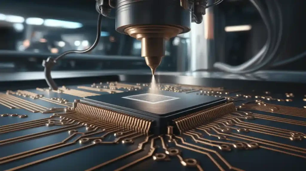
If you’ve ever wondered how electronic devices come to life, it all starts with a well-designed PCB layout. A PCB layout is like the blueprint for your circuit board. It transforms your schematic—a diagram of your circuit—into a physical board that connects all the components. Without it, your electronics project would remain just an idea.
Learning PCB layout design opens up a world of possibilities. You’ll gain skills like managing heat to prevent component failures, reducing electromagnetic interference for cleaner signals, and ensuring your design is easy to manufacture. These are critical for creating reliable and efficient circuit boards. Plus, understanding tools like design rule checking (DRC) helps you catch errors early, saving time and money.
Don’t worry if this sounds complex. With the right tools and a clear design checklist, you can create your first circuit board layout. Start small, experiment, and watch your ideas come to life!
Key Takeaways
A PCB layout helps turn your circuit idea into a working board. It links parts and directs electrical signals.
Begin with a clear diagram and check your parts list (BOM). This avoids expensive errors while designing.
Use easy tools like KiCad or Eagle to make designing simpler. Pick tools that fit your skill level.
Place parts carefully and connect traces properly for a good PCB layout.
Always check design rules (DRC) before finishing. This finds mistakes and ensures it’s ready for manufacturing.
Understanding PCB Layout Design
What is a PCB layout, and how does it work?
A PCB layout is the physical representation of your circuit design. It’s where your ideas take shape on a board, connecting components like resistors, capacitors, and integrated circuits (ICs) through conductive tracks. Think of it as a map that guides electrical signals to flow correctly between components.
Here’s what makes up a typical PCB layout:
PCB Board: The base material, often fiberglass, provides structure and insulation.
Resistors: Control the flow of electricity by adding resistance.
Capacitors: Store and release energy, filter noise, and manage AC/DC signals.
Integrated Circuits (ICs): Tiny chips that perform specific tasks, like processing data.
Conductive Tracks: Copper pathways that carry electrical signals.
Pads: Metal areas where components are soldered onto the board.
Each part works together to ensure your circuit functions as intended. Without a proper layout, your design might fail to operate or face issues like signal interference.
The role of schematics in PCB design
Schematics are the starting point of any PCB design. They act as a blueprint, showing how components connect and interact. A well-drawn schematic ensures your PCB layout is accurate and error-free.
Here’s why schematics are essential:
They detail the connections, components, and signal paths in your circuit.
Following schematic standards keeps your design organized and easy to understand.
A clear schematic reduces errors when transitioning from concept to physical PCB.
By validating your schematic early, you’ll save time and avoid costly mistakes later in the design process.
Overview of essential PCB design tools
Beginner-friendly tools (e.g., KiCad, Eagle, Altium)
Starting with the right tools makes PCB layout design much easier. Tools like KiCad and Eagle are perfect for beginners. KiCad is free and open-source, offering features like schematic drafting, PCB layout, and even 3D visualization. Eagle is affordable and user-friendly, making it a favorite among hobbyists.
Here’s a quick comparison of popular tools:
Software | Key Features | Target Users |
|---|---|---|
KiCad | Free, open-source, supports 3D visualization | Beginners, budget users |
Eagle PCB Tool | Affordable, easy to use, includes auto-routing | Hobbyists, small businesses |
Altium Designer | Professional-grade, extensive libraries, high-speed design | Professionals, advanced projects |
Key features to consider when choosing PCB design software
When picking a PCB design tool, look for features that match your needs. Beginners should prioritize ease of use and affordability. Advanced users might need tools with high-speed design capabilities or extensive component libraries. Compatibility with your operating system is also crucial. For example, KiCad works on Windows, Mac, and Linux, making it accessible to almost everyone.
Choosing the right tool sets the foundation for a smooth PCB design experience.
Preparing to Design a PCB Layout
Validating your schematic and Bill of Materials (BOM)
Before you dive into pcb layout design, you need to validate your schematic and Bill of Materials (BOM). Think of this step as double-checking your shopping list before heading to the store. A well-prepared BOM ensures you have all the components and details needed for a successful pcb design.
Here’s how you can validate your BOM:
Verify that manufacturing part numbers (MPN) and vendor part numbers (VPN) are correct.
Confirm the quantity of each part matches your schematic.
Check that designators in the BOM align with those in your schematic.
Mark any “Do Not Install” (DNI) components to avoid confusion later.
Additionally, keep your BOM updated throughout the design process. This ensures no active parts are left out and avoids costly mistakes during production.
Designing the PCB stack-up
Single-layer vs. multi-layer PCBs
When designing a pcb layout, you’ll need to decide between single-layer and multi-layer PCBs. Single-layer boards are simpler and easier to produce, making them ideal for straightforward designs like LED circuits or basic gadgets. On the other hand, multi-layer PCBs are more complex and can handle advanced designs. They allow for more connections and components in a smaller space, which is perfect for devices like smartphones or laptops.
Multi-layer boards require more planning and advanced manufacturing processes. However, they offer higher performance and durability, making them worth the effort for complex projects.
Choosing materials and layer configurations
The materials you choose for your PCB stack-up play a huge role in its performance. Start with the right laminate—it affects signal losses, heat management, and power handling. For high-frequency boards, go for low-Dk materials. Also, calculate the number of signal, ground, and power layers based on your application needs. This ensures your pcb design can handle the required electrical and thermal demands.
Tip: Carefully design trace geometry, including width and spacing, to maintain uniform impedance in high-speed circuits.
Setting up design rules and constraints
Electrical and manufacturing design rules
Design rules are like the traffic laws of pcb layout design. They guide you on how to place components, route traces, and maintain clearances. Following these rules ensures your board is manufacturable and performs reliably. For example, maintaining adequate spacing between traces prevents electrical failures and improves long-term performance.
Defining trace width, spacing, and via sizes
Trace width and spacing are critical for handling current and avoiding signal interference. Wider traces are better for high-current paths, while proper spacing reduces the risk of short circuits. Similarly, via sizes should match your board’s layer configuration to ensure strong and reliable connections.
By setting up these rules early, you’ll avoid errors during component placement and routing, saving time and effort later.
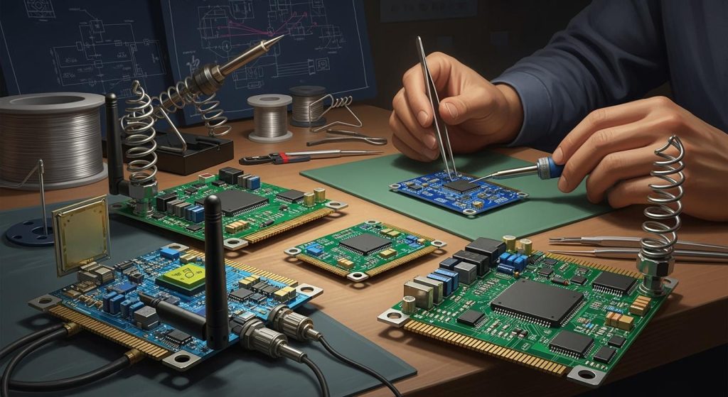
Creating the PCB Layout

Component placement strategies
Prioritizing connectors, power circuits, and precision components
When starting your PCB layout, focus on placing the most critical components first. Begin with connectors since they define how your board interacts with the outside world. Next, position power circuits to ensure efficient power distribution. Precision components, like oscillators or sensors, should follow. These parts are sensitive to noise, so keep them away from high-frequency or power areas.
Here’s a quick checklist to guide your component placement:
Place connectors first to establish external connections.
Add power circuits and ensure they’re close to the power source.
Position precision components in low-noise areas.
Align similar components in the same direction for easier soldering.
By following this order, you’ll create a logical and efficient layout that simplifies the routing process later.
Grouping components by function for efficiency
Grouping components by their function can make your PCB layout more organized. For example, keep all power-related components together and group signal-processing parts in another section. This reduces clutter and makes routing connections easier. It also helps you quickly identify components during debugging or assembly.
Tip: Keep surface-mount devices on one side of the board whenever possible. This streamlines the manufacturing process and reduces costs.
Routing traces and connections
Best practices for signal trace routing
Routing is where your PCB design truly comes to life. To ensure reliable connections, follow these best practices:
Keep signal paths as short as possible to reduce resistance and delays.
Use proper trace widths based on current requirements.
Separate analog and digital signals to avoid interference.
Maintain spacing between traces to prevent crosstalk.
For high-speed signals, use controlled impedance to preserve signal integrity.
Efficient routing minimizes errors and ensures your PCB performs as expected.
Managing power and ground planes
Power and ground planes are essential for stabilizing your PCB. Use the bottom layers for power and ground, while reserving the top layer for signal traces. This arrangement reduces electromagnetic interference and ensures low-impedance return paths.
For mixed-signal designs, isolate analog and digital ground planes to prevent noise. Use stitching vias to connect ground planes and maintain signal integrity. Proper management of these planes ensures your PCB operates smoothly without unexpected issues.
Running design rule checks (DRC)
Common errors detected by DRC
Design rule checks (DRC) are like your safety net. They catch errors that could cause your PCB to fail. Common issues include:
Electrical violations, like short circuits.
Clearance and width constraints.
Vias under surface-mount devices.
Net antennae problems.
Running a DRC ensures your design meets all electrical and manufacturing requirements.
Fixing issues before finalizing the layout
If your DRC flags errors, don’t panic. Use your PCB design software’s rules panel to identify the violations. Investigate the specific rule and adjust your layout to fix the issue. For example, you might need to increase trace spacing or reposition components. Addressing these problems early saves time and prevents costly mistakes during production.
Pro Tip: Always run a final DRC before submitting your design for manufacturing. It’s your last chance to catch errors!
Optimizing Your PCB Layout

Ensuring proper trace width and spacing
Getting the trace width and spacing right is crucial for a reliable PCB layout. It’s not just about fitting everything on the board—it’s about ensuring your design works as intended. Here’s why this matters:
Trace width determines how much current your traces can safely carry. Wider traces handle higher currents without overheating.
Proper spacing prevents electrical arcing and minimizes interference between traces.
Wider spacing also helps with heat dissipation, keeping your PCB cooler during operation.
Additionally, maintaining adequate spacing reduces crosstalk, which can interfere with signal integrity. Always follow your design rules to define the minimum trace width and spacing based on your PCB’s current and voltage requirements.
Tip: Use your PCB design software’s built-in calculators to determine the ideal trace width for your current needs.
Using ground planes to reduce noise
Ground planes are your best friend when it comes to reducing noise in PCB layouts. They provide a low-impedance path for return currents, which improves signal integrity and reduces electromagnetic interference (EMI). Here’s how they help:
Ground planes act as barriers, isolating sensitive circuits from noise.
They enhance power delivery by providing shorter return paths for current.
Large ground planes also spread heat evenly, improving thermal management.
For mixed-signal designs, consider using separate ground planes for analog and digital sections. This reduces crosstalk and ensures cleaner signals.
Pro Tip: Use stitching vias to connect ground planes across layers for better performance.
Power supply considerations
Placement of decoupling capacitors
Decoupling capacitors are essential for stabilizing your power supply. Place them as close as possible to the power pins of your ICs. This minimizes noise and voltage fluctuations, ensuring your components receive clean power.
Tip: Use one capacitor per power pin for critical components to maximize stability.
Managing high-current traces effectively
High-current traces require special attention in PCB design. Wider traces are a must—they reduce resistance and prevent overheating. Proper spacing between these traces is equally important to avoid electrical arcing and thermal interference.
Here are some key considerations:
Wider traces spread heat more effectively, keeping your PCB cooler.
Narrow traces can cause voltage drops, which may affect performance.
Keep high-current traces away from sensitive signal traces to minimize EMI.
By following these practices, you’ll ensure your PCB can handle high currents without compromising performance or reliability.
Finalizing and Ordering Your PCB Design
Generating production files (Gerber, drill files, etc.)
Once your PCB layout is complete, the next step is to generate production files. These files are essential for manufacturing your PCB. Think of them as the instructions your manufacturer will follow to bring your design to life. Here’s a list of the key files you’ll need to prepare:
Gerber files: These define the copper layers, solder mask, and silkscreen.
Drill files: Specify the locations and sizes of holes for vias and components.
Centroid file: Contains data for automated assembly, like component positions and orientations.
Bill of Materials (BOM): Lists all components, including part numbers and quantities.
Fabrication drawings: Provide details like board dimensions and layer stack-up.
Assembly drawings: Show where each component should be placed.
Special requirements documentation: Notes any unique manufacturing needs.
Export these files from your PCB design software and double-check them for accuracy. Missing or incorrect files can delay production.
Reviewing your PCB layout before submission
Before sending your design to a manufacturer, take time for a thorough PCB layout review. This step helps catch mistakes that could lead to costly errors. Common issues to look for include:
Incorrect pin assignments or unconnected nets.
Power and ground problems, like missing connections.
Signal integrity issues, such as poor trace routing.
Missing pull-up or pull-down resistors.
Incorrect component values or inconsistent net naming.
Violations of design rules, like trace spacing or via sizes.
Use your design software’s tools to identify and fix these problems. A careful review ensures your PCB performs as expected.
Choosing a PCB manufacturer
Factors to consider (cost, lead time, quality)
Selecting the right manufacturer is crucial for a successful project. You’ll want to balance cost, lead time, and quality. Start by understanding your specific requirements. Can the manufacturer meet your design needs? Evaluate their capabilities and quality control measures. Look for certifications like ISO 9001 to ensure reliability.
Request quotes from multiple manufacturers to compare pricing. Be cautious of hidden fees that might inflate costs. Also, consider lead times. A faster turnaround might cost more, but it could be worth it for tight deadlines.
Submitting files and placing an order
Once you’ve chosen a manufacturer, submit your production files. Most manufacturers accept Gerber files, drill files, and BOMs. Double-check their submission guidelines to avoid delays. After submitting, confirm your order details, including quantity, material, and delivery timeline.
Tip: Communicate any special requirements clearly to avoid misunderstandings during production.
Designing a pcb layout may seem challenging at first, but breaking it into steps makes the process manageable. Here’s a quick recap to guide you:
Define the concept and functions of your PCB.
Draw a detailed schematic to map out your circuit.
Create a board-level block diagram to plan dimensions and component areas.
Place components logically based on their function.
Route the board nets and prioritize critical connections.
Perform a design rule check (DRC) to catch errors.
Document all fabrication and assembly notes for future reference.
Mastering these steps takes practice, so don’t hesitate to experiment with tools like KiCad or Eagle. The more you design, the more confident you’ll become.
By honing your PCB design skills, you’ll ensure signal integrity, improve reliability, and avoid costly redesigns. Plus, a well-designed PCB directly impacts the functionality and manufacturability of your project. Whether you’re building a simple gadget or a complex device, these skills will set you apart as a capable designer.
Tip: Start small, stay curious, and enjoy the process of bringing your ideas to life!
FAQ
What is the best way to start designing a PCB layout?
Start with a clear schematic. Double-check your connections and components. Then, use a PCB design tool to create your layout. Follow a checklist to ensure you don’t miss critical steps like setting design rules or validating your schematic.
How do I choose between single-layer and multi-layer PCBs?
Single-layer PCBs are great for simple projects. They’re cost-effective and easy to manufacture. Multi-layer PCBs work better for complex designs with limited space. They allow more connections and better performance but require advanced planning and higher manufacturing costs.
Why are design rule checks (DRC) important?
DRC helps you catch errors before manufacturing. It ensures your PCB meets electrical and manufacturing requirements. Running a DRC saves time and money by preventing issues like short circuits, improper trace spacing, or unconnected nets.
What are the benefits of using ground planes?
Ground planes reduce noise and improve signal integrity. They provide a low-impedance path for return currents and help with thermal management. For mixed-signal designs, separating analog and digital ground planes minimizes interference.
How do I prepare files for PCB manufacturing?
Export production files like Gerber and drill files from your design software. Include a Bill of Materials (BOM) and fabrication notes. Double-check everything to ensure accuracy. Missing or incorrect files can delay production or lead to errors.