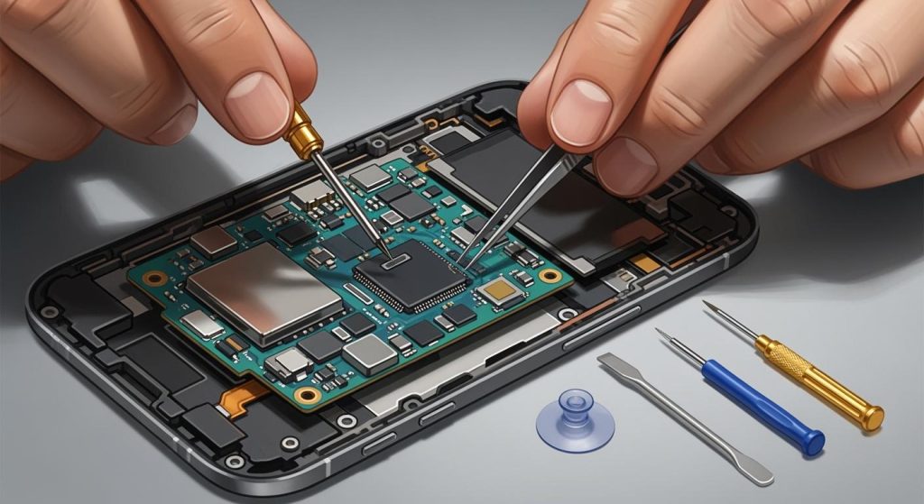
A well-designed power supply PCB is essential for ensuring the safety and reliability of your electronic systems. Poor design choices can lead to serious consequences. For example: insufficient power trace width causes voltage drops, risking component failure; rapid switching introduces noise, corrupting data in sensitive ICs; and narrow traces result in overheating, damaging components. Uneven power distribution can also cause malfunctions or overheating, reducing system reliability. By addressing these issues, you can enhance performance and extend the lifespan of your devices.
Key Takeaways
Placing parts correctly is very important. Put high-current parts close to the power input to avoid voltage loss.
Good heat control stops overheating. Use heat sinks and thick copper lines to help remove heat.
Grounding keeps the circuit stable. A good ground plane reduces noise and makes the circuit work better.
Use wide power lines to stop voltage loss. Short and wide lines lower resistance and keep power steady.
Handle EMI/EMC issues early. Use shields and filters to reduce interference and follow rules.
Poor Component Placement in Power Supply PCB Layout

Why Proper Placement is Crucial
The placement of components in a power supply pcb layout directly impacts the performance, efficiency, and safety of your design. Proper placement ensures smooth current flow, minimizes noise, and prevents overheating. For example, placing high-current components like voltage regulators near the power input reduces voltage drops. Similarly, keeping sensitive components, such as microcontrollers, away from noisy power components avoids interference. By organizing your pcb into functional areas, you can improve both performance and troubleshooting.
Another critical factor is thermal management. Components that generate heat, such as power transistors, should be positioned near heat sinks or thermal vias. This arrangement optimizes heat dissipation and prevents damage. Additionally, placing connectors along the edges of the board simplifies assembly and maintenance. These principles not only enhance the reliability of your power supply layout but also ensure compliance with safety standards.
Common Placement Errors in Power Supply PCBs
Engineers often make mistakes that compromise the functionality of switching power supplies. One common error is placing critical components too far apart, which increases trace length and loop area. This can lead to noise issues and signal degradation. Another frequent mistake is failing to position decoupling capacitors close to IC power pins, reducing their filtering effectiveness. Overlapping components or insufficient clearances can also cause solder bridges and shorts, jeopardizing safety.
Heat-generating components are sometimes placed too close together, leading to poor thermal performance. EMI-sensitive components, such as oscillators, may be positioned without adequate shielding, resulting in interference. Inefficient placement can also complicate routing, making the pcb harder to test and troubleshoot. Avoiding these errors is essential for a reliable power supply pcb layout.
Strategies for Effective Component Placement
To optimize your power supply layout, follow these best practices:
Divide the pcb into functional areas to reduce interference.
Place high-current components near the power input and away from the edges.
Keep signal lines short and direct to minimize attenuation.
Position heat-generating components near heat sinks or thermal vias.
Place decoupling capacitors close to their associated ICs for effective filtering.
Separate sensitive components from noisy ones to prevent coupling.
Using tools like Altium Designer can further enhance your pcb design. Its 3D visualization feature helps verify component orientation, while its collaborative tools streamline teamwork. By adhering to these strategies, you can create a power supply pcb layout that is efficient, safe, and easy to maintain.
Inadequate Thermal Management in Power Supply Design
The Impact of Poor Heat Dissipation
Effective thermal management is critical in power supply PCB design. Without proper heat dissipation, components can overheat, leading to irreversible damage. High temperatures accelerate material aging, reducing the reliability of your design. Overheating can also cause signal integrity issues, resulting in noise and performance degradation. In extreme cases, thermal runaway may occur, where rising temperatures lead to catastrophic failure.
Temperature fluctuations pose additional challenges. Repeated heating and cooling cycles create mechanical stress, which can weaken solder joints and cause microfractures. This stress may lead to cracks or delamination in PCB materials, further compromising the system. Excessive heat can also trigger safety concerns, such as fire hazards, making thermal regulation a top priority in your design.
Frequent Thermal Management Mistakes
Many designers overlook key aspects of thermal regulation in power supply PCBs. One common mistake is failing to position heat-generating components near heat sinks or thermal vias. This oversight can result in hotspots that damage sensitive parts. Another frequent error is underestimating the importance of material selection. Using low-conductivity materials limits heat dissipation, increasing the risk of overheating.
Improper component placement also contributes to thermal issues. Placing high-power components too close together restricts airflow, reducing cooling efficiency. Neglecting to use thick copper traces or thermal via arrays can create localized heating, further stressing the PCB. These mistakes not only compromise performance but also jeopardize safety.
Best Practices for Managing Heat in Power Supply PCBs
To improve heat dissipation in your power supply design, consider these strategies:
Use heat sinks made of aluminum or copper to draw heat away from components.
Incorporate cooling fans to enhance airflow and remove heat quickly.
Design thick copper traces to spread heat evenly and reduce hotspots.
Add thermal via arrays to connect PCB layers and distribute heat effectively.
Select materials with high thermal conductivity, such as metal-core PCBs or ceramics, for better heat management.
Optimize your PCB layout by spacing components to improve airflow and cooling.
By implementing these techniques, you can ensure reliable power regulation and enhance the safety of your design. Proper thermal management not only extends the lifespan of your PCB but also prevents costly failures.
Improper Grounding in PCB Design
The Role of Grounding in Power Supply PCBs
Grounding plays a vital role in ensuring the reliability and performance of your power supply PCB. A well-designed ground plane provides a low-impedance path for return currents, which minimizes voltage drops and fluctuations. This is essential for maintaining stable voltage levels across the board. Proper grounding also enhances noise immunity, shielding sensitive circuits from electromagnetic interference (EMI). By offering a continuous reference plane, grounding ensures clear signal return paths, reducing the risk of data corruption or performance degradation.
In addition to improving electrical performance, grounding contributes to the safety of your design. It prevents stray currents from damaging components or causing malfunctions. A robust grounding strategy is especially critical in complex systems where multiple circuits interact. Without it, your PCB may suffer from noise issues, signal distortion, or even complete failure.
Typical Grounding Errors
Improper grounding is one of the most common mistakes in PCB design. Ground loops often occur when multiple return paths exist, leading to unwanted noise and interference. These loops can be avoided by shortening traces and carefully placing ground planes. Another frequent error is neglecting to place bypass capacitors near power supply pins. This oversight can result in ground bounce and voltage spikes, which compromise the stability of your power supply.
Routing sensitive signals across split ground planes is another mistake to avoid. This creates discontinuities in the return path, increasing EMI and signal distortion. Additionally, failing to maintain routing on a single layer can complicate return paths, especially for high-speed signals. These errors not only degrade performance but also make troubleshooting more challenging.
Techniques for Proper Grounding in Power Supply Layouts
To achieve effective grounding in your PCB design, follow these best practices:
Keep ground planes uniform to minimize voltage drops and improve signal integrity.
Place the ground plane directly below the signal plane to reduce return path lengths.
Use separate ground planes for high and low-voltage sections to reduce crosstalk.
Implement a copper pour ground fill and connect it with vias for uniformity.
Place bypass capacitors close to power supply pins to reduce ground bounce.
Avoid routing high-speed signals across voids in the ground plane.
Use single-point grounding for low-frequency designs and multipoint grounding for high-frequency systems.
By applying these techniques, you can enhance the performance and reliability of your power supply PCB. Proper grounding not only ensures stable operation but also protects your design from noise and interference.
Insufficient Power Trace Design in Power Supply PCBs
Why Power Trace Design Matters
Power traces are the lifelines of your PCB, carrying current to components and ensuring stable operation. Poorly designed traces can lead to voltage drops, overheating, and even component failure. For power supply circuits, maintaining power integrity is critical. Short and wide traces reduce resistance and minimize electromagnetic interference (EMI), which is especially important in high-speed designs. Proper trace design also ensures uniform power distribution, preventing some components from being underpowered while others are overloaded. Without reliable power traces, your power conversion system may fail to deliver consistent performance, especially in demanding applications like ac to dc conversion.
Common Power Trace Design Issues
Designers often encounter several issues when creating power traces for PCBs. Narrow traces with high resistance can cause voltage drops, leading to critical component failures. Overheating is another common problem, as narrow traces cannot handle high current demands. Switching noise from rapid power supply transitions can introduce jitter in sensitive ICs, while uneven power distribution may cause malfunctions. Additionally, neglecting to use a solid ground plane increases noise coupling, further degrading performance. These issues not only compromise the efficiency of your power conversion system but also shorten the lifespan of your PCB.
Tips for Designing Reliable Power Traces
To design effective power traces, follow these strategies:
Use PCB design calculators to determine the appropriate trace width based on current and copper thickness.
Minimize trace lengths to reduce resistance and EMI.
Place high-current components near the power input to prevent voltage drops.
Route high-current paths on the outer layers of the PCB for better heat dissipation.
Use multiple vias for high-current traces to ensure adequate capacity.
Isolate sensitive signals from power traces to avoid interference.
Incorporate thermal vias and heat sinks to manage heat effectively.
By implementing these practices, you can enhance the reliability of your power supply PCB. Proper trace design ensures stable power conversion, reduces EMI, and prevents overheating, making your design robust and efficient.
Overlooking EMI/EMC in Isolated Power Supply Design
Understanding EMI/EMC in Power Supply PCBs
Electromagnetic interference (EMI) and electromagnetic compatibility (EMC) are critical factors in isolated power supply PCB design. EMI refers to unwanted noise or signals that disrupt the performance of electronic systems, while EMC ensures that your design operates reliably without interfering with other devices. High-frequency switching regulators, common in isolated power supplies, often generate EMI through conducted and radiated emissions. These emissions can compromise the functionality of sensitive components and lead to regulatory compliance failures.
You must address EMI/EMC early in the design process. Identify sources of EMI, such as common-mode currents, parasitic ringing, and switching noise. For instance, common-mode currents can arise from discontinuous grounds or parasitic coupling, while parasitic ringing often occurs during low-load conditions. Understanding these sources helps you implement effective mitigation strategies, ensuring your PCB meets safety and EMC standards.
Common EMI/EMC Design Pitfalls
Many designers overlook key aspects of EMI/EMC, leading to costly redesigns. One common mistake is improper trace routing, which increases noise and signal degradation. For example, using sharp trace bends or excessive vias can introduce parasitics and disrupt signal integrity. Another frequent issue is neglecting electrostatic discharge (ESD) testing, which is essential for compliance with CE standards. Failures often occur at chassis ground connections, especially at I/O connectors.
Ignoring the impact of high-frequency switching can also result in significant problems. Higher PWM frequencies amplify EMI, making it harder to control. Without proper shielding or controlled impedance, your PCB may fail EMC testing, delaying production and increasing costs. To avoid these pitfalls, prioritize EMI considerations throughout the design process.
Methods to Reduce EMI/EMC Problems in Isolated Power Supplies
You can mitigate EMI/EMC issues in isolated power supply designs by following proven strategies:
Reduce the area between power lines and their return paths to lower impedance.
Use low-pass filters to suppress conducted EMI at the power supply output.
Minimize common-mode currents by optimizing ground pour near switching sections.
Implement shielding with conductive materials to block radiated EMI.
Arrange PCB layers to include a continuous ground plane for better EMC performance.
Group components by signal type (e.g., analog, digital) to reduce interference.
Place decoupling capacitors close to IC power pins to manage power rail noise.
By applying these methods, you can ensure your PCB design meets EMI/EMC requirements. Effective EMI management not only enhances the reliability of your isolated power supply but also prevents costly failures and regulatory issues.
Avoiding common mistakes in power supply PCB design is essential for creating reliable and efficient systems. Errors like neglecting testing, insufficient trace width, and poor power distribution can lead to voltage drops, overheating, and performance issues. Careful planning and adherence to best practices, such as proper grounding, effective thermal management, and optimized component placement, ensure stable operation and longevity.
By implementing strategies like using decoupling capacitors, managing EMI, and designing robust power planes, you can enhance your PCB’s performance. These practices not only improve current capacity and reduce voltage drops but also simplify power distribution and minimize electromagnetic interference. Thoughtful design choices ultimately save time, reduce costs, and prevent failures in your power supply systems.
Take the time to refine your design process. A well-planned PCB ensures consistent performance and protects your investment in the long run.
FAQ
1. What is the most critical factor in power supply PCB design?
The most critical factor is ensuring proper power distribution. You must design wide traces, minimize resistance, and maintain stable voltage levels. This prevents overheating, voltage drops, and component failures. Proper grounding and EMI management also play a key role in ensuring reliable performance.
2. How can you prevent overheating in power supply PCBs?
You can prevent overheating by using heat sinks, thermal vias, and thick copper traces. Position heat-generating components near cooling elements. Optimize airflow by spacing components properly. Selecting materials with high thermal conductivity also helps dissipate heat effectively.
3. Why is grounding important in PCB design?
Grounding ensures stable operation by providing a low-impedance path for return currents. It minimizes noise, prevents voltage fluctuations, and shields sensitive components from EMI. Proper grounding also enhances safety by protecting your PCB from stray currents and electrical malfunctions.
4. How do you reduce EMI in power supply designs?
To reduce EMI, use low-pass filters and shielding materials. Minimize the loop area between power lines and return paths. Place decoupling capacitors close to ICs. Group components by signal type and maintain a continuous ground plane for better electromagnetic compatibility.
5. What tools can help improve PCB design?
PCB design software like Altium Designer or KiCad can help. These tools offer features like 3D visualization, trace width calculators, and EMI analysis. They simplify layout optimization and ensure compliance with design standards, making your PCB more reliable and efficient.
Tip: Always test your PCB design under real-world conditions to identify and fix potential issues before production.