PCB Design Preparation
1. Information to be provided with hardware C
●Accurate schematic diagrams, including paper and electronic files and error-free network tables.
● An official BOM with component codes. the hardware engineer should provide a DATASHEET or physical object for components that are not in the package library and specify the order in which the pins are defined.
● Provide a general layout of the PCB or the location of important units and core circuits. Provide PCB structure diagrams, which should indicate the shape of the PCB, mounting holes, positioning components, prohibited areas, and other relevant information.
2. Basic design requirements before design
● High-current components and networks of 1A or more.
● Important clock signals, differential signals, and high-speed digital signals.
● Analog small signals and other easily disturbed signals.
● Other special required signals.
3. Special request notes
● Differential distribution lines, networks requiring shielding, characteristic impedance networks, equal delay networks, etc.
● Prohibited wiring zones for special components, solder paste offsets, solder resist openings, and other structural special requirements.
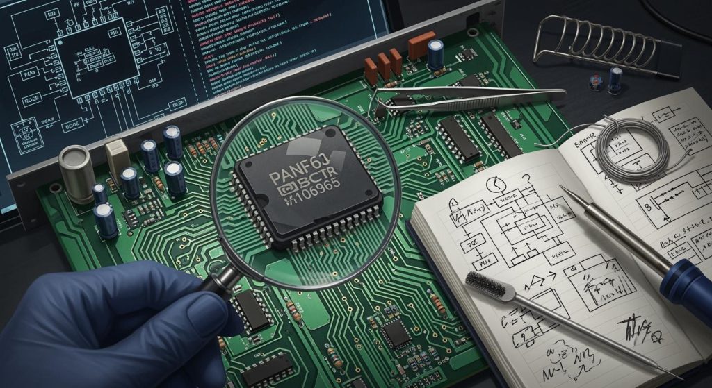
● Read schematics carefully to understand the circuit architecture and to understand the operating conditions of the circuit.
● Confirm the critical networks in the PCB and understand the design requirements for high-speed components based on thorough communication with hardware engineers.
Design Process
1. Packaging of fixed components
● Open the network table and browse through all packages to make sure that the packages of all components are correct and that the component library contains the packages of all components, and that all the information in the network table is capitalized, so that one side is loaded with problems or the PCB BOM is not continuous, and that the specific naming of the components is named in accordance with the company’s standardized naming. Standard components are all packaged in the company’s unified component library.
● For packages that do not exist in the component library, the hardware engineer should provide the component DATASHEET or the physical object to build the library by the person who is specialized in building the library and ask the other party to confirm.
2. Establish PCB board frame
● Create a PCB file according to the PCB structure drawing, or the corresponding template, including mounting holes, no-wiring zones, and other related information.
● Dimensioning. The exact structure of the PCB should be indicated in the drilling layer and closed dimensioning is not possible.
3. Import network table
● Import the netlist and troubleshoot all loading issues, each EDA software is different, check the tutorials on how to handle this.
● If you are using EDA software, the netlist must be imported more than twice (without any prompting message) to confirm that the import is correct.
4 .PCB Layout
● The first step is to determine the reference point. Generally, the reference point is set at the intersection of the left and bottom border lines (or the intersection of the extension lines) or at the first pad of the printed board’s insert.
Once the reference point is determined, the component layout and wiring will be based on this reference point. A 10-25 MIL grid is recommended for layout.
● Secure and lock all elements with positioning requirements first, as required.
● Basic principles of layout:
① Follow the principle of putting the difficult before the easy and the big before the small.
② Layout: You can refer to the schematic and rough layout provided by the hardware engineer and place the main original devices according to the signal flow pattern.
③ The total connecting lines are as short as possible, with the shortest critical signal lines.
④ Strong signals, weak signals, high voltage signals and weak voltage signals should be completely separated.
⑤ High-frequency components should be adequately spaced.
⑥ Separate analog and digital signals.
● Symmetrical layouts should be adopted wherever possible for circuit parts of the same structure.
● Optimize the layout according to the criteria of even distribution, balanced centre of gravity and aesthetically pleasing layout.
● Components in the same row should be aligned in the X or Y direction. Polarized discrete components in the same row should also be aligned in the X or Y direction to facilitate production and debugging.
● Components should be placed in a way that facilitates debugging and maintenance, no small components should be placed on the side of large components, and there should be enough space around the components that need to be debugged. Heat generating components should have enough space for heat dissipation. Thermal components should be kept away from heat generating components.
● Dual in-line components should be more than 2 mm away from each other.
- mm. Small SMD components such as resistors and capacitors should be more than 0.7 mm away from each other. The outside of the pads of SMD components should be more than 2 mm from the outside of the pads of neighbouring cartridge components. Plug-in devices must not be placed within 5 mm of a crimped component. SMD components must not be placed within 5 mm of the soldering surface.
● The decoupling capacitor of the integrated circuit should be as close as possible to the power supply pin of the chip, with high frequency as the principle of closest proximity. The shortest circuit should be formed between it and the power supply and ground.
● Bypass capacitance should be evenly distributed around the IC.
● When laying out components, components using the same power supply should be considered to be placed together as much as possible to facilitate future power supply splitting.
● The placement of resistive and capacitive devices used for impedance-matching purposes should be rationalized according to their properties.
The layout of matching capacitors and resistors should be clearly defined, and the terminal matching for multiple loads must be placed at the farthest end of the signal.
●The layout of the matching resistor should be close to the driving end of the signal, and the distance is generally no longer than 500
● Adjust the characters. All characters must not be on the upper disk to ensure that the character information can be clearly seen after assembly. All characters should be consistent in the X or Y direction. The size of characters and silk leads should be uniform.
● Place the MARK point of the PCB.
5. PCB wiring
●Prioritization of cabling
① Principle of loose density: Start wiring from the device with simple connection relationship on the printed board, and start wiring from the area with the loosest connection to regulate the individual state.
② Core priority principle: for example, DDR RAM and other core parts should be prioritized wiring, similar signal transmission lines should provide a dedicated layer, power, ground loop. Other minor signals should be considered as a whole, and should not conflict with the key signals.
③Key signal line priority: power supply, analog small signals, high-speed signals, clock signals and synchronization signals and other key signals priority wiring.
● Ground circuit rules.
Loop minimum rule, that is, the signal line and its loop constitutes the ring area should be as small as possible, the ring area should be as small as possible, the smaller the ring area, the less radiation to the outside world, receiving the outside world of the ten disturbances is also smaller. For this rule, in the ground plane division, to take into account the distribution of the ground plane and the important signal alignment, to prevent the problems brought about by the Sandin ground plane slots, etc.: in the double-layer board design, in the case of leaving enough space for the power supply, should be left behind to fill in the part of the ground with reference to allow the increase of some of the necessary holes, will be connected to both sides of the signal effectively connected to the meter, some key signals try to isolate the use of ground for some of the higher frequency design, need special consideration. For some higher frequency designs, special consideration should be given to the ground plane signal loop, and it is recommended to use multilayer boards.
● Scrambling control:
Mutual interference between different networks on the PCB caused by long parallel wiring is mainly due to the role of distributed capacitance and distributed inductance between parallel lines. The main measure to overcome the interference is to increase the distance between the parallel wiring and follow the 3W rule.
● Shielding protection:
Corresponding to the ground loop rules, in fact, is also to minimize the signal loop area, more for some of the more important signals, such as clock signals, synchronization signals: for some particularly important, especially high-frequency signals, should be considered using the copper-axis cable shielding structure design, that is, the cloth line up and down the left and right land line isolation, but also to consider how to effectively allow the shielding of the ground and the actual ground plane is effectively combined.
● Rules for alignment direction control:
Adjacent layers of the alignment direction into an orthogonal structure to avoid different signal lines in adjacent layers into the same direction, in order to reduce unnecessary inter-layer interference; when due to the structural limitations of the board it is difficult to avoid the situation, especially when the signal rate is high, should be considered with the ground plane isolation of the wiring layer, the ground signal line isolation of the signal line.
● Impedance matching rules:
The width of the wiring should be consistent across the same network. Variations in the width of the wiring can cause unevenness in the characteristic impedance of the wiring and reflections at higher transmission speeds, which should be avoided as much as possible in the design. Under certain conditions, such as connector lead wires, BGA package lead wires and similar constructions, it may not be possible to avoid variations in line width, and the effective length of the intermediate inconsistencies should be minimized.
- Alignment length control rules:
Alignment length control rules that is, the short line rule, in the design should try to make the wiring length as short as possible, in order to reduce the interference problems caused by the length of the alignment, especially some important signal lines, such as the clock line, be sure to put its oscillator in a place very close to the device. For driving multiple devices, it should be decided what kind of network topology to use according to the specific situation.
- Chamfering rules:
Sharp and right angles should be avoided in PCB design, generating unwanted radiation as well as poor process performance. All line to line angles should be ≥ 135°.
- Integrity rules for power and ground layers:
For areas with a high density of conduction holes, care should be taken to avoid holes interconnecting in the dug-out areas of the power and ground layers, creating a division of the planar layer, which can damage the integrity of the planar layer and, in turn, lead to an increase in the loop area of the signal lines in the ground layer.
- 3W Rule:
In order to reduce the tampering between the lines, should ensure that the line spacing is large enough, when the center of the line is not less than 3 times the line width, it can maintain 70% of the electric field does not interfere with each other, known as the 3W rule. If you want to achieve 98% of the electric field does not interfere with each other, you can use the 10W rule.
●Rule 20H:
Since the electric field between the power and ground layers is variable, electromagnetic interference is radiated outward at the edges of the board. This is called the edge effect. It is possible to shrink the power supply layer inward so that the electric field is conducted only within the confines of the ground layer. In terms of one H (the thickness of the dielectric between power and ground), an inward contraction of 20H will confine 70% of the electric field to the grounded edge; an inward contraction of 100H will confine 98% of the electric field.
Setup Rules
1. Arranging the stacking order
● In high-speed digital circuits, the power and ground layers should be as close together as possible, with no wiring arranged in between.
All wiring layers are as close to a plane as possible, with the ground plane preferred as the isolation layer.
● In order to minimize interference between signals, the signal directions of adjacent wiring layers should be perpendicular to each other, and if it is not possible to avoid the same direction, then the overlapping of signals in the same direction of adjacent signal layers should be avoided by all means.
● You can set up several impedance layers according to the requirements. The impedance layers should be labeled clearly as required, pay attention to the selection of the reference layer, and arrange all the signals with impedance requirements on top of the impedance layer.
2.Set the line width, line spacing
● When the average signal current is relatively large, it is necessary to consider the relationship between line width and current, for details, refer to the following table, the current-carrying table for copper-platinum of different thicknesses and widths.
3.Setting up the over-hole
The following table can be used for the setting of perforation pads and hole diameters.