At present, electronic products have penetrated into every corner of our lives, and their products cover communications, medical, computer peripheral audio-visual products, toys, household appliances, military products, etc. Regarding the PCBA welding of electronic products, manual welding is generally used in the sample stage. The advantage of manual welding is that it is low-cost and can be done with a soldering iron. If a few sample boards are welded by the machine, the value of the sample is not enough to cover the cost of the machine.
In order to improve the efficiency of manual welding and the accuracy of component welding, wonderfulpcb DFM has launched a visual welding tool that interacts with the BOM list and PCB diagram. This tool can also help SMT factories check and count component materials and find repair points. Visual BOM interactive welding tools are efficient and practical, which is really a blessing for SMT factories and PCB engineers.
Visual BOM interactive welding tool – application scenario
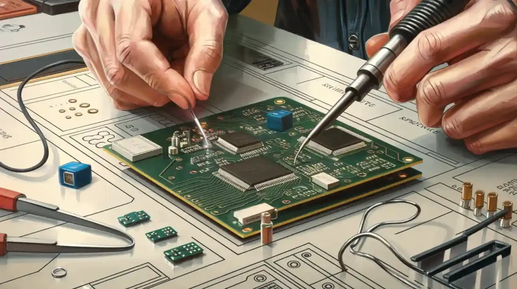
Engineer hand welding
What pain points of manual welding have been solved by the visual BOM interactive welding tool?
- When manually soldering components, there is a risk of soldering the wrong components due to the large number and variety of components used. Using the visual BOM interactive soldering tool can avoid the problem of soldering the wrong components.
- The way to manually solder is to print out the assembly drawing and solder the components according to the assembly drawing, but the specific information of the components cannot be intuitively seen when using the assembly drawing for soldering. All the information of the visual BOM interactive soldering tool is clear at a glance and can completely replace the assembly drawing.
- Use the visual BOM interactive soldering tool to solder components, and the design graphics can be zoomed in and out to view in different ways. Components can be soldered clearly and correctly.
- In the settings, you can set the display of one-pin mark to avoid the problem of soldering the wrong direction of components. You can also set the display of soldered and empty sticker marks to avoid confusion about components during soldering.
SMT factory
What conveniences do the visual BOM interactive soldering tool help SMT factories improve?
- When IQC engineers check the material points for storage, they can use the visual BOM interactive soldering tool to accurately find out whether there are extra materials or less materials.
- When IQC engineers take materials to check pads, they can search for specification values or packages to locate all pad positions on the PCB board where this material is pasted.
- When repairing SMT wrong materials, the wrong material positions can be quickly screened to facilitate material removal and repair.
- When clearing the SMT order, you can check the empty paste option to quickly mark the position number that needs to be empty due to insufficient material.
Visual BOM interactive welding tool – Preparation before use
PCB/ODB file
Use wonderfulpcb DFM to open the design file, drag the PCB file or ODB file into the software operation window, or click the file point in the menu bar to open. After opening the design file, use the visual BOM interactive welding tool in the menu bar (Tools → Visual BOM Interaction).
Gerber/Coordinate/BOM file
Use wonderfulpcb DFM to open the design file, drag the Gerber file into the software operation window, and also need to load the coordinate and BOM files. After completing the assembly analysis, use the visual BOM interactive welding tool in the menu bar (Tools → Visual BOM Interaction).
Visual BOM interactive welding tool – Function details
Filter function
After entering the visual BOM interactive welding tool, you can filter a device according to the position number, package, and specification value at the arrow mark on the left, and filter the patch components and plug-in components at the arrow mark on the right.
Tool link sharing
When using the visual BOM interactive welding tool, if you need to share it with others, you can click “Copy Link” or “WeChat Scan Code” to share it and send it to colleagues or partners.
Export function
If the visual BOM interaction needs to be saved as a document during use, the HTML web document can be exported as an offline document. Just click “Export”. If you need to save the image, click the top or bottom layer to save the corresponding layer image. When exporting the image, you can choose a transparent background. When the exported image is blurry, you can set the image size.
Component list statistics
Component list statistics, count the top components, bottom components, and component types separately. The number of pads counts the SMD pads and plug-in pads separately. When the soldered components and the empty and unsoldered components are marked, the percentage is analyzed with the unsoldered components to facilitate the viewing of the proportion of unsoldered devices.
Page split screen mode
When the BOM file interacts with the PCB design file, it can be viewed on a split screen. The mark “1” shows the BOM components in rows according to the component type, the mark “2” shows the BOM components in rows according to the position number, the mark “3” shows the entire BOM table, the mark “4” shows the BOM table and the design drawing in split screens on the left and right, and the mark “5” shows the BOM table and the design drawing in split screens on the top and bottom.
Top and bottom layer viewing mode
When using the visual BOM interactive welding, the design graphics can view the top layer and the bottom layer separately. Mark “1” to view the top layer alone, mark “2” to view the top layer and the bottom layer at the same time, and mark “3” to view the bottom layer alone.
Display settings
The display settings of the visual BOM interactive welding tool can set the display background color and whether to display it on full screen. The display categories that can be set include bit number, specification value, pad, silk screen, and one-pin identification of the device. The design graphics can be adjusted to view at any angle. The identification color can be set when checking the soldered, empty, and unsoldered parts.
Welding viewing operation
When soldering the board, check the position of the bit number corresponding to the PCB graphics. The label “1” can set the list to be viewed, and the columns that do not need to be viewed can be left blank. Label “2” marks the soldered components with a √ mark, label “3” marks the empty and unsoldered components with a √ mark, label “4” switches the row with the up and down keys on the keyboard, and the space bar marks the soldered or empty and unsoldered components with a √ mark. The middle mouse button in the graphics window can be used to scroll the graphics to zoom in and out, and the left mouse button can be held down to drag the graphics. Label “5” is the graphics display window. When you need to display the soldered components, select soldered in the graphics setting. The soldered device graphics are marked in green.