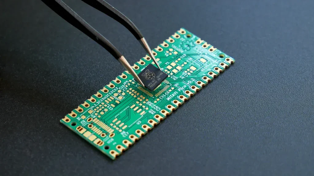
A PCB stack-up is how layers are arranged in a circuit board. These layers include conductive and insulating materials. This setup is very important for how well electronics work. A good stack-up helps signals stay clear and power flow smoothly. It also keeps the board cool and lasts longer. Planning it right can save money when making the board. As gadgets get more advanced, a smart stack-up is key for strong circuits and durable products. Knowing this helps you design boards that work well and are easy to make.
Key Takeaways
A good PCB stack-up makes signals clear and reduces noise. Put signal layers close to ground layers for better performance.
A proper stack-up helps control power and manage heat. This keeps devices working well and stops them from overheating.
Picking the right number of layers and materials is important. Balance cost and quality to make useful and affordable PCBs.
Don’t make mistakes like skipping impedance control or heat management. These problems can cause expensive production troubles.
Work with manufacturers early when designing. Their advice can make production easier and improve the stack-up design.
What Is a PCB Stack-Up?

Definition of PCB Stack-Up
A PCB stack-up is how layers are arranged in a circuit board. These layers include copper for carrying electricity and materials for insulation. The stack-up affects how signals move, how power spreads, and how heat is managed. It is very important for the board’s performance and structure. For fast electronics, the stack-up treats signal paths like special lines to work better and avoid problems.
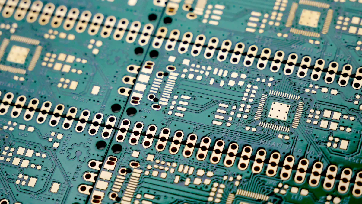
Layers in a PCB Stack-Up
Signal Layers
Signal layers are where electricity moves between parts of the board. These layers connect different parts of the circuit with traces. The way they are placed affects how well signals work. In boards with many layers, signal layers are often between ground and power layers to reduce noise and interference.
Power and Ground Planes
Power layers send voltage across the board to give parts energy. Ground layers help complete electrical loops and act as a reference. Together, they make the board handle electricity better and lower resistance. In fast circuits, these layers can also act like small capacitors to improve performance.
Insulating Layers
Insulating layers keep conductive layers apart to stop short circuits. These layers are made from strong materials like FR-4, which handle heat and pressure well. They also make the board stronger and last longer in tough conditions.
Role of PCB Stack-Up in PCB Functionality
The stack-up design affects how the board works. A good stack-up keeps signals clear, spreads power well, and handles heat. It also protects the board from outside noise and interference. For fast and advanced circuits, a smart stack-up is needed for the best results.
Why Does PCB Stack-Up Matter?
How It Affects Signals
A good stack-up keeps signals working properly. Signals in a PCB can face problems like noise or loss. Placing signal layers next to ground layers helps fix this. This setup controls impedance, so signals move without issues. For fast devices, this is very important since small problems can cause big issues.
Putting layers in the right order also reduces crosstalk. Crosstalk happens when signals from one layer mess with another. A six-layer PCB stack-up improves signals by separating them with ground layers. This design keeps signals strong, even in complex boards.
How It Helps Power Flow
The stack-up design decides how power spreads in the PCB. Power and ground layers work together to give steady voltage to parts. A good stack-up lowers noise and stops power flow problems. This is very important for fast devices where small changes can cause trouble.
Smart layer placement also helps manage heat better. This stops the board from getting too hot and keeps it working well. A well-planned stack-up makes the system more reliable and helps all parts work smoothly.
Why It’s Important for Heat Control
Heat control is another reason stack-up design matters. Stronger devices make more heat, which can damage parts. Insulating layers in the stack-up help spread heat and stop hot spots.
New stack-up designs can make heat control even better. Using materials that spread heat well keeps the board cool. This protects parts and makes the board last longer. Good heat control is key for keeping modern PCBs working and durable.
Influence on Manufacturing Costs and Complexity
How you design your PCB stack-up affects costs and difficulty. A good stack-up plan saves money and makes production easier. Poor planning can cause higher costs and delays.
Adding more layers to a PCB makes it harder to build. Each layer needs careful alignment and bonding. This requires special tools and skilled workers, which increases costs. For example, making a four-layer PCB costs less than an eight-layer one. But cutting layers without planning can hurt signals and performance.
The materials you choose also affect the cost. Better materials last longer and improve signals but cost more. Special materials for heat or signal control can raise expenses. You need to balance quality with your budget.
Stack-up design also changes how long manufacturing takes. Complex designs with many layers need more testing and fixing. This slows production and raises labor costs. Simple designs that still work well speed up the process.
Vias, which connect PCB layers, also matter. Blind or buried vias don’t go through the whole board. These need extra steps to make, which adds cost.
A smart stack-up design reduces problems during manufacturing. A clear plan lowers mistakes, speeds up production, and controls costs. This helps your PCB work well without going over budget.
Key Things to Think About in PCB Stack-Up Design
Deciding the Number of Layers
The number of layers affects how your PCB works. Decide this early in the design process. Simple boards often use two layers. Complex boards, like in fast devices, need four or more layers. More layers improve signals by cutting noise and interference. They also separate power and ground layers better.
Think about the pros and cons of adding layers. More layers cost more and are harder to make. Fewer layers might hurt how the board works. A good balance keeps the board working well and within budget.
Picking Materials for PCB Stack-Up
The materials you pick affect how strong and good your PCB is. Most boards use FR-4, which is cheap and reliable. It insulates well and handles heat. For faster devices, you might need better materials like Rogers laminates. These help signals move better and lose less energy.
Also, think about how thick the insulating layers are. Thicker layers separate conductive layers better, helping signals. But they can make the board thicker. Always choose materials that fit your design needs.
Controlling Impedance in Stack-Up Design
Impedance control helps signals move smoothly without problems. This is very important for fast circuits. To do this, arrange layers carefully in your stack-up. Put signal layers next to ground layers to keep impedance steady.
The thickness of insulating layers and material type also matter for impedance. Use design tools to adjust these during planning. Good impedance control makes signals better and avoids problems like crosstalk.
Avoiding Common Stack-Up Design Mistakes
Mistakes in stack-up design can cause problems and delays. Knowing these errors helps you make a better PCB.
Ignoring Signal Integrity
Not placing signal layers near ground planes causes issues. This can lead to signal loss and interference. Always keep signal layers close to ground planes for better signals.Overlooking Impedance Control
Forgetting to manage impedance can harm fast signals. Some designers skip checking insulating layer thickness or use wrong materials. Use tools to check impedance fits your design.Using Too Few Layers
Cutting layers to save money can hurt performance. Without power and ground planes, noise increases, and reliability drops. Pick enough layers to balance cost and function.Poor Thermal Management
Ignoring heat control can damage parts. Use materials that spread heat well and plan heat paths. This keeps your PCB working under heavy use.Choosing Inappropriate Materials
Cheap materials may fail under heat or weaken signals. Pick materials that suit your PCB’s needs and conditions.
Tip: Work with your manufacturer early. Their advice can help you avoid mistakes and make production easier.
Fixing these mistakes improves your PCB stack-up and speeds up production.
Benefits of a Well-Designed PCB Stack-Up
Better Electrical Performance
A good PCB stack-up helps signals move smoothly. Arranging layers carefully reduces noise and interference. This keeps signals clear and strong. Placing signal layers near ground planes improves signal quality. It also stops problems like crosstalk, where signals mix and cause issues.
For fast devices, a smart stack-up keeps impedance steady. This avoids signal loss and keeps circuits working well. Whether your PCB is simple or complex, a good stack-up boosts its electrical performance.
Stronger Heat and Mechanical Strength
A smart stack-up helps control heat and makes the board stronger. Devices create heat, and too much can harm parts. Insulating layers spread heat evenly to stop hot spots.
Good designs also make the board tougher. Studies show:
Better heat control improves how devices work.
Clearer signals make boards stronger.
Stronger boards last longer in tough conditions.
By focusing on these, your PCB stays reliable even under stress.
Saves Money in Manufacturing
A well-planned stack-up lowers costs when making the board. Using fewer layers cuts material costs but keeps performance good. Fewer layers also make production faster and cheaper.
Picking the right materials affects cost too. FR-4 is cheap and works for most boards. For advanced boards, better materials cost more but last longer.
A clear design reduces mistakes during production. This means less fixing and faster delivery. A cost-effective stack-up saves money and makes building easier.
Easier Design and Debugging
A good PCB stack-up makes design and debugging simpler. Planning layers well creates a clear structure. This saves time and avoids stress during development.
How Stack-Up Design Helps PCB Layout
A clear stack-up shows how signals and power move. You can easily see where signals go and how power flows. This helps prevent mistakes like crossing wires or bad connections.
For example, putting signal layers near ground layers reduces noise. This setup keeps signals steady and easy to manage. You won’t waste time fixing signal problems later.
Tip: Use design tools to plan your stack-up. Programs like CAD help you map layers and spot issues early.
Debugging Becomes Simpler
When issues happen, a smart stack-up makes fixing them easier. You can quickly find problems in specific layers or parts. Signal issues, like noise or mismatched impedance, are easier to solve with a clear layer order.
A good stack-up also lowers the chance of hidden problems. Separating power and ground layers keeps voltage steady. This stops random errors that are hard to figure out.
Why It Helps You
🛠 Quick fixes: Clear layers make it easy to find and fix problems.
📋 Better teamwork: A neat stack-up is like a guide for your design.
💡 More reliable: Fewer mistakes mean your PCB works better with less rework.
Focusing on stack-up design makes your work easier and your PCB more dependable.
A good PCB stack-up is very important for reliable boards. It keeps signals clear, controls heat, and lowers costs. Planning the stack-up early helps avoid mistakes and speeds up production.
Tip: Work with your manufacturer while designing. Their advice can help you make a stack-up that works well and stays affordable.
Focus on your stack-up design to create PCBs that last and perform well.
FAQ
What is the purpose of a PCB stack-up?
A PCB stack-up arranges layers in a circuit board. It helps signals stay clear, controls heat, and spreads power well. A smart stack-up also lowers costs and makes boards more reliable.
How does a PCB stack-up affect signal integrity?
A good stack-up reduces noise and interference. Putting signal layers close to ground layers keeps signals clear. This setup also controls impedance, so signals move smoothly without problems.
Can a poor stack-up design increase costs?
Yes, bad designs can cause delays and cost more. Complicated or uneven designs need extra materials and work. A simple, clear stack-up lowers mistakes and speeds up production.
What materials are commonly used in PCB stack-ups?
FR-4 is the most used material. It insulates well and handles heat. For advanced boards, materials like Rogers laminates improve signals and last longer.
Why is thermal management important in PCB stack-ups?
Thermal management stops parts from overheating and breaking. Insulating layers spread heat evenly across the board. Heat-spreading materials keep the board cool and working longer.
Tip: Talk to your manufacturer early in the design process. Their advice helps you make a better and cheaper stack-up.