One of the most fundamental considerations in PCB design is determining how many routing layers, ground planes, and power planes are needed to meet the circuit’s functional requirements. The stack-up design of the PCB is usually a compromise, taking various factors into account. Below are the key principles for PCB stack-up design.
stack-up Planning

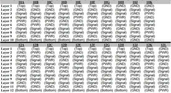
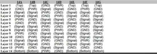
Outer Layers with GND and PWR: These layers are primarily used for routing and shorting out traces. For HDI (High-Density Interconnect) applications, the second layer is often a signal layer used for routing traces between fine-pitch BGA components. In this HDI application, manufacturers typically use laser drilling for controlled-depth drilling to access the second layer.
Balancing Layers: All stack-ups must have a balanced layer stack-up from the PCB’s central line to minimize or eliminate warping. The type and thickness of the prepreg (pre-impregnated material) must be determined before starting the CAD layout.
Manufacturing Considerations: It is necessary to conduct a stack-up analysis with the manufacturer to determine the copper weight, prepreg material, and core thickness before CAD layout, ensuring controlled impedance.
Material Thickness:
- 1.6mm FR4 material is used for stack-ups with 2–16 layers.
- 1.8mm FR4 is used for stack-ups with 10–20 layers.
- 2.3mm FR4 is used for stack-ups with 10–32 layers.
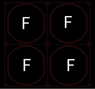
Common PCB Thicknesses:
- A. 0.8mm (0.031″)
- B. 1.0mm (0.040″)
- C. 1.6mm (0.062″)
- D. 1.8mm (0.070″)
- E. 2.3mm (0.090″)
- F. 3.2mm (0.125″)
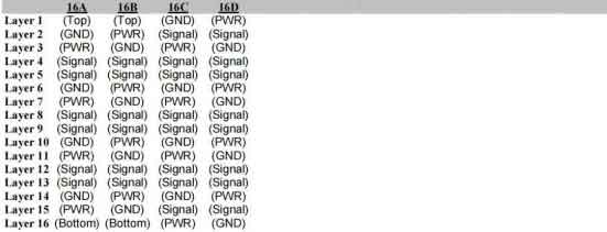
stack-up Design Principles
Layer Segmentation
In multi-layer PCBs, the layers typically include signal layers (S), power layers (P), and ground layers (GND). Power and ground layers are usually contiguous and provide a low-impedance return path for current flowing through adjacent signal traces. Signal layers are mostly positioned between these power or ground reference plane layers. The top and bottom layers of a multi-layer PCB are typically used for placing components and a small amount of routing.
Determining a Single Power Reference Plane
Decoupling capacitors should only be placed on the top and bottom layers of the PCB. The routing, pads, and vias connecting to these capacitors can significantly affect their performance. Therefore, it is important to ensure that the traces connecting to the decoupling capacitors are as short and wide as possible, with vias connected to these traces being as short as possible.
Determining Multiple Power Reference Planes
Multiple power reference planes are divided into separate regions, each providing different voltage levels. If the signal layers are adjacent to these multiple power planes, the signals on these layers may encounter poor return paths, which could negatively impact signal integrity. Therefore, high-speed digital signal routing should be kept away from multiple power reference planes.
Determining Multiple Ground Reference Planes (Ground Planes)
Multiple ground reference planes provide a low-impedance return path for currents, helping to reduce common-mode EMI (Electromagnetic Interference). Ground and power planes should be tightly coupled, and signal layers should also be tightly coupled with the adjacent reference planes.
Designing Routing Combinations
The combination of layers that a signal trace crosses is referred to as a “routing combination.” The best routing combination design avoids return currents from flowing between different reference planes. Ideally, the return current should flow from one point on a reference plane to another point on the same plane.