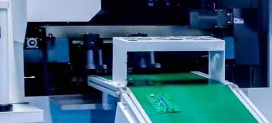
The proper placement of electronic components on a PCB (Printed Circuit Board) is a critical factor in reducing soldering defects. A well-planned layout plays a significant role in the overall quality of the assembly. When designing the layout, components should be placed in areas with minimal bending and internal stress, and their distribution should be as uniform as possible. This is especially important for components with high thermal conductivity, where large PCBs should be avoided to minimize expansion and contraction. Poor layout design can adversely affect both the tradeability and stability of the PCB.
In many cases, designers, in an effort to maximize the use of available space, may place components as close as possible to the board’s edges. This practice, however, can present significant challenges in manufacturing and PCBA assembly. In some cases, it can even lead to problems during soldering or assembly.
The Risks of Placing Components Near PCB Edges
1. Edge Milling Issues
When components are placed too close to the edge of the PCB, the milling process during board shaping can remove the component’s pads. Generally, the distance between the pad and the board edge should be at least 0.2mm. If the pad is too close to the edge and is milled off, it will prevent the component from being soldered correctly during assembly.

2. V-CUT Issues during Panelization
If the edge of the PCB is being processed using V-CUT during panelization, components should be placed even farther from the edge. The V-CUT blade typically cuts through the middle of the board, and components must be at least 0.4mm away from the edge to prevent the blade from damaging the pads. Otherwise, the V-CUT blade could damage the pads, making it impossible to solder the components.
3. Interference with Equipment
When components are placed too close to the edge of the PCB, they may interfere with the operation of automated assembly equipment, such as wave soldering or reflow soldering machines. This can lead to production delays or even malfunctioning equipment.
4. Potential Damage to Components
The closer components are placed to the edge of the PCB, the greater the potential for interference with assembly equipment. For example, large components such as electrolytic capacitors, which are taller than other components, should be placed farther from the edges of the PCB to prevent them from being damaged during assembly.
5. Component Damage During Depanelization
After the product assembly is complete, the PCB panel will need to be depanelized. If components are placed too close to the edge, they may be damaged during the separation process. This damage can be intermittent, making it difficult to detect and troubleshoot later.
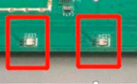
Real Case of PCB Edge Component Damage
Issue Description
In the SMT placement process of a certain product, it was found that the LED lights were placed too close to the edge of the board, making them prone to being damaged during production.
Impact of the Problem
During production, transportation, and the DIP process through the machine, the LED lights were frequently damaged, affecting the functionality of the product.
Consequences and Extension
The solution required redesigning the PCB layout to move the LED lights inward from the edge, which also necessitated modifications to the structure and the light guide column. This caused significant delays in the project development cycle.