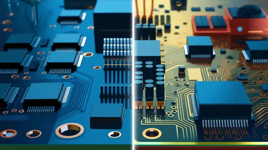
Switch PCBs play a crucial role in electronics, enabling easy control of electrical circuits. To design switch PCB effectively, careful planning is essential, as decisions made during this process can influence up to 80% of production costs. The global PCB market expanded significantly, growing from $7.1 billion in 1995 to over $60 billion by 2012, highlighting the increasing demand for well-thought-out designs. Mastering how to design switch PCB, manufacture, and replicate them can minimize errors and accelerate production. However, replicating PCBs raises ethical concerns, making it vital to focus on creating innovative designs while respecting the intellectual property of others.
Key Takeaways
Learn what the switch PCB needs to do and how it works. Pick the right switch type so it works well for your project.
Use easy-to-learn PCB design software like KiCad or Eagle. These programs make designing easier and help you avoid errors.
Test and check your PCB design carefully to find problems early. This saves time and money when making the PCB.
Get all the design files ready for making the PCB. Include Gerber files and leave enough space to avoid assembly issues.
Follow the rules about copying PCB designs. Use open-source designs to learn and create without breaking any laws.
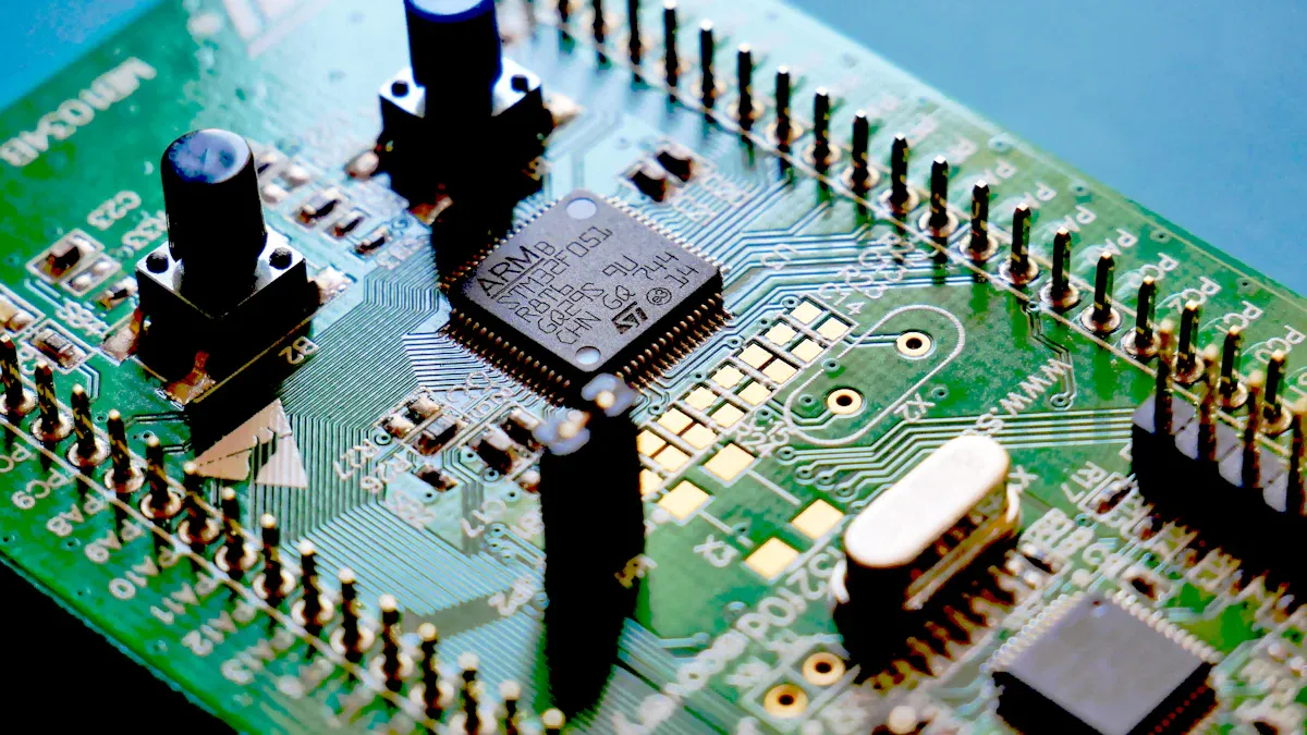
Design Switch PCB

Understanding Electrical and Mechanical Requirements
To design a switch PCB, know its electrical and mechanical needs. These needs help the PCB work well and fit the device. First, pick the right switch for your project. For example, toggle switches are good for power control, and push buttons are great for user input. Below is a table showing common switch types and their uses:
Switch Type | Description | Use Case |
|---|---|---|
Toggle Switches | Switches with a lever that stays in place | Turning power on or off |
Slide Switches | Small sliders for power modes or settings | Changing device settings |
Push Buttons | Pressable switches for temporary circuit connection | Resetting or user input |
Dip Switches | Tiny toggles grouped for settings | Adjusting configurations |
Keypad or Keyboard Switches | Buttons that sense key presses | Operating control panels |
SPST | Simple on/off switch | Basic circuit control |
SPDT | Switch directing input to one of two outputs | Controlling complex circuits |
DPDT | Switch managing two circuits at once | Handling advanced circuits |
Think about current rating, durability, and how hard it is to press. Power switches need to handle more current. Tactile switches should last through many uses. Place switches where users can easily reach them.
Choosing PCB Design Software
Using the right software makes designing easier. Tools like KiCad, Eagle, and Altium Designer are popular. They help with schematics, layouts, and testing. Some programs have pre-made parts to save time. If you’re new, pick software that’s easy to learn and has good support.
Creating the Schematic and Layout
A schematic is like a map for your PCB. It shows how parts connect and helps find mistakes early. Use it to plan where switches and other parts go. For example, put capacitors near power pins and keep ground areas clear to avoid problems. After the schematic, move to the layout. Arrange parts to reduce signal issues and save space. Make sure grounding is good and add safety features like ESD protection. A good layout improves performance and makes fixing or building easier.
Testing and Simulating the PCB Design
Testing your switch PCB ensures it works well in all conditions. Simulation tools can predict how it will act before making it. These tools find problems and improve the design for better results.
First, test the electrical parts of your design. Use software to check voltage, current, and signals. Make sure switches work as they should and the circuit runs properly. SPICE simulators are great for this job.
Mechanical testing is also important. Your PCB must handle stress like shaking, shocks, and weight. Rules like MIL-STD and IPC guide these tests. For example, vibration tests check if switches work in tough conditions.
Thermal testing checks how your PCB handles heat. Hot or cold temperatures can cause problems. Standards like IPC-TM-650 and MIL-STD-202G help test these situations. If your PCB works in extreme heat or cold, thermal tests are a must.
Chemical testing looks at how your PCB reacts to harmful substances. This is key for designs used in harsh places. HALT and HASS tests show how your PCB ages over time. These tests predict long-term performance.
Other tests include checking power loads, electromagnetic safety, and resistance to dust, water, or radiation. Running these tests helps improve your PCB and meet industry rules.
Testing and simulating save time and money. They lower mistakes during production and ensure your PCB works well in real life.
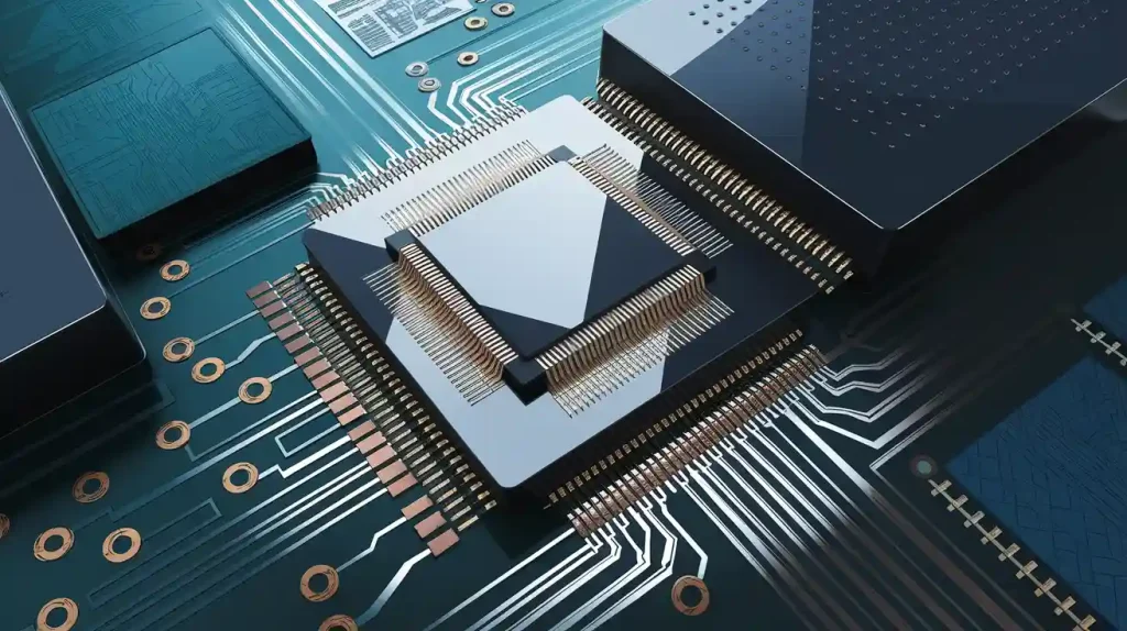
Manufacturing a PCB
Preparing Design Files for Fabrication
Getting your design files ready is very important. To make the PCB correctly, give the manufacturer all needed files. Include Gerber files, drill files, and a netlist. These files tell the manufacturer how to build your PCB. Missing or extra files can slow things down.
Think about how easy it is to make your design. For example, leave enough space between parts to avoid problems. Use wide enough traces to carry current safely. The table below shows some helpful tips:
DFM Consideration | Best Practice | Impact |
|---|---|---|
Component Spacing | Leave enough room | Avoids assembly problems |
Trace Width | Use wide traces for current | Stops overheating and signal loss |
Via Placement | Avoid too many vias in key paths | Keeps signals strong |
Panelization | Arrange boards smartly | Saves money and materials |
Solder Mask | Keep clearances correct | Stops solder from connecting wrongly |
Also, include a layer stack diagram to show the PCB’s structure. Add drill files with exact details for making holes. These steps help turn your design into a real PCB smoothly.
Selecting a PCB Manufacturer
Picking the right manufacturer is very important. Choose one with certifications like ISO 9001 for quality or IPC A-600 for board standards. The table below explains some certifications:
Standard/Certification | Description |
|---|---|
ISO 9001 | Ensures good quality management systems. |
IPC A-600 | Sets rules for high-quality printed boards. |
RoHS | Makes sure no harmful materials are used. |
Ask for samples to check their work. See if they follow IPC rules and use good technology. Talking to their past clients can also help you decide.
Overview of the PCB Fabrication Process
Making a PCB turns your design into a working board. First, your design is printed onto a copper board. Extra copper is removed, leaving only the needed parts. Holes are drilled for components and connections, then plated for electricity flow.
Next, a solder mask is added to protect the board. Labels are printed for easy assembly. The board is then cut to size and checked for quality.
Quality checks are very important. The first batch is inspected to match the design. Metrics like First Pass Yield (FPY) show how well the process works. A high FPY means fewer mistakes and less rework.
By knowing these steps, you can make sure your PCB is made well and meets standards.
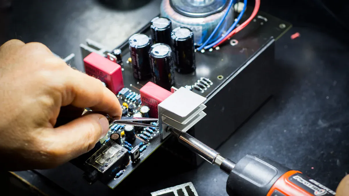
Assembly and Quality Assurance
The assembly process turns your PCB design into a working board. This step includes adding parts, soldering, and checking if it works. Quality assurance (QA) makes sure the board is reliable and meets standards.
Assembly Process
During assembly, parts like resistors, capacitors, and switches are added. Small parts use Surface Mount Technology (SMT). Bigger parts, like dome switches, use Through-Hole Technology (THT). Placing switches and parts correctly is very important. Bad placement or poor soldering can cause problems.
To keep things consistent, use Standard Operating Procedures (SOPs). These steps guide workers during assembly. Fixing repeated problems improves the process. Good supplier management ensures high-quality parts are used.
Quality Assurance Techniques
QA checks the board for mistakes and tests its performance. Common methods include:
Technique | Description |
|---|---|
Automated Optical Inspection | Cameras take pictures to find misplaced parts or bad soldering. |
In-Circuit Testing | Checks if each part works and finds issues like short circuits. |
Functional Testing | Makes sure the board works as it should under test conditions. |
Inspection reports show problems and how they were fixed. These reports include results from visual checks, AOI, functional tests, and X-rays.
Reports include findings from visual checks, AOI, functional tests, and X-rays, listing problems and fixes.
A strong QA process ensures the board works well. It also lowers the chance of problems in the final product.
Final Steps
After QA, the board is cleaned and packed. Labels help identify switches and other parts. This step gets the board ready for the final product.
Copying a PCB Switch: Ethical and Technical Aspects
Legal Rules for PCB Design Copying
Knowing the law is key when copying a PCB switch. Intellectual property laws protect original designs and their creators. Breaking these laws can lead to fines or lawsuits. Check if the PCB design is patented or copyrighted before copying. If it is protected, ask the creator for permission.
Courts use legal standards to decide expert testimony in toxic cases. These rules can help understand intellectual property issues in PCB copying.
Learning these legal rules helps you avoid breaking the law. Talking to a lawyer can clarify if your actions follow intellectual property laws.
Steps to Reverse Engineer a PCB Switch
Reverse engineering means taking apart a PCB to learn how it works. This needs skill and careful work. Below are the steps:
Step | What to Do |
|---|---|
1 | Find parts like resistors, capacitors, and chips. |
2 | Get PCB samples and scan them for details. |
3 | Map connections between parts based on PCB type. |
4 | Use machines to quickly identify components. |
5 | Collect documents and check part numbers. |
6 | Use a multimeter to confirm connections. |
7 | Show data visually and create reports. |
These steps help you understand the PCB design. Use this knowledge wisely and don’t copy designs without permission.
Ethical Issues in PCB Design Copying
Copying PCB designs brings up ethical problems. Learning through reverse engineering is fine, but copying without permission is unfair to creators. It can hurt the industry by reducing creativity and innovation.
Focus on making your own designs instead of copying others. Open-source PCB designs are a good option. They are free to use and promote teamwork. Using open-source designs lets you learn while respecting intellectual property.
Think about how your actions affect the electronics community. Ethical choices protect creators and encourage trust and new ideas.
Exploring Open-Source PCB Designs
Open-source PCB designs are great for learning. These designs are free to use, change, and study. They help you save time and learn professional design methods.
You can find open-source PCB designs on sites like GitHub, OSHPark, and PCBWay Community. These sites have many designs, from simple circuits to advanced boards. Many include guides to help you understand the designs.
Benefits of using open-source PCB designs include:
Cost Savings: Use designs without paying extra fees.
Learning Opportunity: Learn industry methods and good practices.
Collaboration: Work with others and share knowledge.
💡 Tip: Always check the license terms. Some designs need you to credit the creator or share changes under the same license.
To begin, download a design that fits your project. Open it in PCB software and study the layout. Look at how parts are placed and connected. This hands-on method improves your PCB skills.
Learning from Existing PCB Designs
Existing PCB designs are great for learning. They show how experts solve problems. This can help you improve your designs.
Start by taking apart old devices. Look at the PCB and find its parts. Use a multimeter to trace connections and learn how the circuit works. Write down what you find for future use.
Compare different designs to learn more. For example, see how they manage power or signals. Use a table to organize your findings:
Feature | Design A | Design B |
|---|---|---|
Power Distribution | Wide traces, few vias | Narrow traces, many vias |
Component Placement | Compact, logical grouping | Spread out, less organized |
🔍 Note: Reverse engineering is useful but respect intellectual property. Use what you learn to create, not copy.
By studying and analyzing designs, you can learn PCB basics. This will help you make better and more reliable PCBs for your projects.
Making a switch PCB needs careful steps. First, know the electrical and mechanical needs. Then, create schematics and test the design. For manufacturing, prepare files, pick a good manufacturer, and check quality during assembly.
Being ethical in PCB work is very important. Respect others’ designs and make your own ideas. If studying other designs, get permission or use open-source ones.
💡 Tip: Use open-source PCB designs to learn and try new ideas. They are great for building skills and being creative.
FAQ
What does a switch PCB do?
A switch PCB helps control and connect circuits in devices. It makes signals flow smoothly and offers an easy way to use electronics. You’ll see them in keyboards, control panels, and gadgets needing input or power control.
What software is good for designing a switch PCB?
Top choices are KiCad, Eagle, and Altium Designer. These tools help with schematics, layouts, and testing. Beginners should pick software that’s simple to use and has helpful support.
How can you test a switch PCB design?
Use tools like SPICE to check electrical performance. Test voltage, current, and signals. Do mechanical tests for strength and thermal tests for heat handling. These steps make sure your PCB works well in real life.
Is copying a PCB design allowed?
Copying a PCB design without approval might break the law. Check if the design is patented or copyrighted. If it is, get permission or use open-source designs to stay legal.
Where can you get open-source PCB designs?
Sites like GitHub, OSHPark, and PCBWay Community have free open-source PCB designs. They offer simple to advanced layouts with guides for learning and editing.
💡 Tip: Always check the license rules before using or changing open-source designs.