Router PCBs are very important in today’s networking devices. They help send data and make sure devices communicate smoothly. You might ask why these PCBs matter so much. It’s because they handle tricky routing jobs while keeping signals clear.
New trends show why they are becoming more important:
Automation and smart factories are changing how PCBs are made.
Smaller devices need HDI technology for better routing.
Cars use special PCBs for safety systems and electric engines.
Green efforts push makers to use eco-friendly materials.
5G networks need high-frequency PCBs with accurate routing.
Knowing these trends helps you see why router PCBs are key to the future of technology and networking.
Key Takeaways
Router PCBs help devices share data easily in networks.
Use short paths and good grounding to improve signals.
Pick materials like FR4 or Rogers for heat and frequency needs.
Test and check quality often to make sure PCBs work well.
Learn about copyright laws before copying PCBs to stay legal.
Router PCB Design Basics
Principles of router PCB design
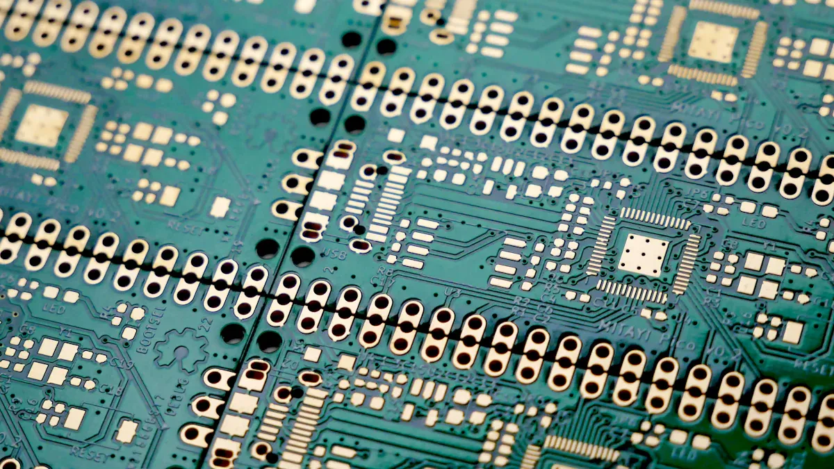
To design router PCBs well, follow key rules. Match signal traces to the nets in your schematic. Keep traces short and direct for better signals. Route traces horizontally on one side and vertically on the other. This reduces interference between signals.
Modern rules like IPC-2221 guide you on materials, schematics, and heat control. These rules help avoid problems with manufacturers and improve PCB quality. Also, using a shared ground plane under signal traces lowers impedance. This is very important for fast designs.
Tip: Put high-speed parts near the ground plane for better results.
Tools for designing router PCBs
Good tools make PCB design easier. Altium Designer is a top choice. It combines design and documentation tools in one program. This makes work faster and simpler. It also has tools to handle tricky routing tasks automatically.
Mechanical details like trace shapes, via holes, and board size must meet IPC and ASME rules. Altium Designer helps you follow these rules and create documents from your layout. This saves time and ensures your design meets industry standards.
Design considerations for networking applications
Networking needs careful PCB designs. High-frequency signals need good impedance control. Big power planes help keep impedance low for steady performance. Use tools like Sketch Routing to handle tough routing tasks smartly.
Heat control is very important for networking devices. Leave enough space between parts to avoid overheating. Following IPC rules during design makes your PCBs more reliable. By focusing on these points, you can make strong and efficient router PCBs.
PCB Manufacturing Process for Routers

Choosing and Preparing Materials
The first step is picking the right materials. Router PCBs need materials that handle heat and high frequencies. FR4 is popular because it’s strong and affordable. For advanced designs, Rogers or Teflon materials work better for signals.
Materials must be prepared carefully. Clean copper boards to remove dirt and grease. This helps layers stick well during manufacturing. Good preparation lowers mistakes and improves PCB quality.
Steps to Make a PCB
Making a PCB has many steps. Each step ensures the router PCB works well. Here’s a simple list:
Design the PCB and make a schematic.
Create a Bill of Materials (BOM).
Do routing design and important checks.
Make photo film and print inner layers.
Align layers and drill holes.
Add copper plating and image outer layers.
Etch the board and add a solder mask.
Finish assembly.
Each step needs to be precise. For example, drilled holes must match the design exactly. Following these steps makes sure the PCB is reliable.
Assembly and Testing for Quality
Assembly adds parts to the PCB. Machines called pick-and-place make this faster and more accurate. These machines place parts in the right spots, reducing mistakes.
Testing is very important in PCB making. Buying parts from trusted suppliers avoids fake components. Tests check if the PCB works well in real-life conditions. These tests ensure the router PCB is reliable.
By focusing on quality at every step, you can make strong router PCBs that meet industry needs.
Copying Router PCBs: Ethical and Technical Insights
Legal considerations in PCB copying
Copying PCBs brings up serious legal issues. You need to know about intellectual property (IP) laws before copying any design. Many PCBs are protected by patents, copyrights, or trade secrets. Copying without permission can cause legal trouble.
Tip: Always check if the PCB design is open-source or needs a license. This helps you avoid breaking any laws.
Some countries have stricter IP rules than others. Learn the laws in your area to stay safe. Following ethical practices keeps you legal and builds trust in your work.
Reverse engineering techniques
Reverse engineering means studying a PCB to recreate its design. This needs special tools and skills. First, carefully remove parts from the board. Next, trace the connections and layers using software or by hand.
Advanced tools like X-ray imaging can show hidden layers in complex PCBs. After collecting all the details, you can make a schematic and copy the design. This process takes accuracy and patience.
Note: Reverse engineering is only allowed if you have permission or if the design isn’t protected by IP laws.
Risks and challenges in replication
Copying a router PCB has risks. A big challenge is making sure the copy works like the original. Small mistakes in tracing or materials can cause signal problems or overheating.
Another risk is using fake parts. These can lower the quality and reliability of your PCB. Testing the copied board in real conditions is important to find and fix problems.
By knowing these risks, you can copy PCBs carefully and professionally.
Best Practices for Router PCB Projects
Tips for efficient design and manufacturing
Making router PCBs needs good planning and careful work. Start by organizing your component libraries well. This makes designing faster and reduces mistakes. Use smart methods to improve performance and reliability. For example, keep trace lengths short to boost signals and lower impedance issues.
Placing parts correctly is very important. Put capacitors close to power supplies to keep them steady and avoid signal problems. Use block diagrams to plan and group parts logically. Before finishing your design, check it with DFM and DFT reviews. These checks make sure your design is ready for making and testing.
Managing heat is also key. Use heat sinks or thermal vias to stop overheating. Following these steps helps you design better and make PCBs smoothly.
Ensuring high-quality production
Making great PCBs needs accuracy and focus. Pick the right profiling method for your needs. Laser cutting is very precise but costs more. Punching is cheaper for big batches, while routing works for many materials.
Profiling Method | Precision | Production Volume | Material Compatibility | Cost Effectiveness |
|---|---|---|---|---|
Laser Cutting | High | Medium | Thick materials | High cost |
Punching | Medium | High | Standard materials | Low cost |
Routing | Medium | Low | Many materials | Medium cost |
V-Cut | Low | High | Simple shapes | Lowest cost |
Testing is very important to check if the PCB works well. Early testing finds problems and fixes them quickly. Good documentation helps solve issues and share knowledge. By focusing on these steps, you can make PCBs that meet industry rules.
Avoiding common mistakes in PCB copying
When copying PCBs, avoid errors for better results. Place parts properly to stop interference and meet needs. Smart heat designs help control temperature and keep the PCB working well.
Prepare all needed files for manufacturers to avoid mistakes. Talk to your manufacturer about any process changes. This saves money and reduces design errors. By doing these things, you can copy PCBs correctly and avoid big problems.
Router PCBs are very important for networking devices. Making them needs good planning and careful work. You should pick the right materials, design smart layouts, and check quality to make them work well. Using eco-friendly materials is now a big part of making electronics.
Important points to remember:
Designing for easy production (DFM) makes work faster and better.
Hiring others to make PCBs can save money on hard tasks.
Reducing harm to the environment is key in today’s PCB making.
Reminder: Following fair rules in PCB copying respects intellectual property and builds trust. Always check if you have permission before copying or studying designs.
Good tools and guides make your work easier. They help you design great PCBs that meet industry rules. Using these tools can lead to success in your router PCB projects.
FAQ
What does a router PCB do?
A router PCB helps devices share data in a network. It makes sure signals move smoothly between devices. Without it, devices can’t send or receive data properly.
Can you make a router PCB without fancy tools?
Yes, you can use free tools like KiCad for simple designs. But advanced tools like Altium Designer make hard designs easier. They also help you follow industry rules.
How do you pick the best material for a router PCB?
Pick materials based on your design needs. FR4 is good for normal designs. Rogers or Teflon is better for high-frequency uses. Always check heat and signal needs when choosing.
Is copying a router PCB always wrong?
Copying is okay if you have permission or it’s open-source. Most designs are protected by intellectual property laws. Always check the rules before copying to stay safe.
What mistakes happen in router PCB making?
Mistakes include bad trace routing, wrong materials, and no testing. These can cause signal problems or overheating. Careful planning and testing can stop these issues.