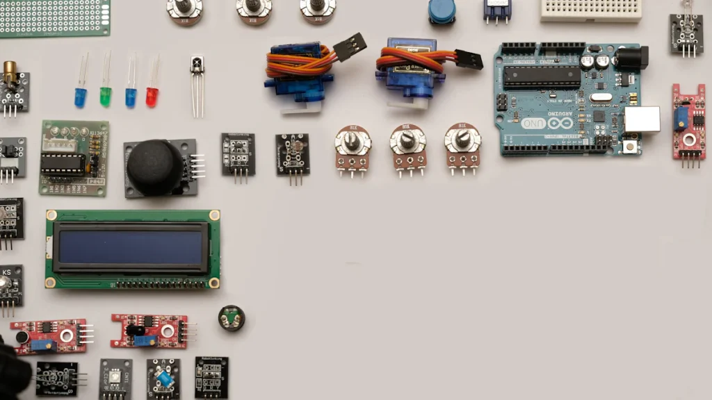
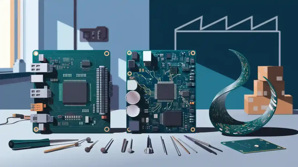
Printed Circuit Board (PCB) design forms the backbone of modern electronics. It involves creating a layout that connects electronic components, ensuring devices function seamlessly. Understanding PCB design is crucial for beginners because it lays the foundation for building reliable and efficient electronic systems. Without this knowledge, even the most innovative ideas may fail to materialize.
Mastering PCB design opens doors to successful projects. For instance, musical instruments like synthesizers and robotics projects such as drones rely on well-crafted PCBs. Additionally, advancements like AI and IoT integration have made PCB design more critical than ever. These technologies optimize layouts and automate processes, enhancing performance and efficiency.
Key Takeaways
Learning PCB design is important for making good electronics. It helps build strong and successful projects.
Use standard design rules to make sure your PCB works well. This lowers mistakes and makes it more reliable.
Testing your PCB design is very important. It finds problems early, saves time, and cuts production costs.
Placing parts correctly and routing well makes PCBs work better. Put similar parts together and keep paths short to avoid problems.
Pick the right PCB design software for your project. Check its features, ease of use, and support to choose wisely.
Understanding PCB Design Basics
What Is a Printed Circuit Board (PCB)?
A printed circuit board (PCB) is the foundation of most electronic devices. It provides a platform to connect and support electronic components, enabling them to work together seamlessly. The structure of a PCB consists of several layers, each serving a specific purpose:
The substrate offers mechanical support and determines the board’s electrical properties.
Copper layers form the conductive pathways, ensuring electrical signals flow between components.
The solder mask protects the copper traces and prevents short circuits during assembly.
The silkscreen layer displays labels and symbols, helping you identify component placements and orientations.
This layered design ensures that a PCB can handle complex circuits while maintaining reliability and efficiency.
Key Components of a PCB
Every PCB includes essential components that perform specific functions. Resistors control the flow of electricity, while capacitors store and release energy, filtering noise and stabilizing power. Integrated circuits (ICs) act as the brain of the circuit, performing tasks like processing data or amplifying signals.
You will also find active components, such as transistors and ICs, which amplify or switch signals. Passive components, like inductors, resistors, and capacitors, regulate the flow of electricity without amplifying it. Together, these components enable the circuit board to perform its intended function.
Types of PCBs and Their Applications
PCBs come in various types, each suited for specific applications:
Single-Sided PCBs: Found in low-cost devices like calculators.
Double-Sided PCBs: Used in smartphones and power monitoring systems.
Multilayer PCBs: Common in computers and medical equipment due to their compact design.
High-Density Interconnect (HDI) PCBs: Ideal for miniaturized electronics like wearables.
Industries such as telecommunications, automotive, and healthcare rely on specialized PCBs. For example, high-frequency PCBs are used in communication systems, while aluminum-backed PCBs are preferred for LED lighting due to their heat dissipation properties.
Why PCB Design Is Essential in Electronics
PCB design plays a vital role in the development of modern electronics. Without a well-designed printed circuit board, electronic devices would struggle to function reliably. You rely on PCBs to ensure that your devices perform as intended, whether it’s a smartphone, a medical device, or an IoT gadget.
A good PCB design determines the functionality, reliability, and performance of your electronic products. It allows you to manage the complexity of modern devices, especially those with advanced features like wireless connectivity. For example, IoT devices often require compact and efficient circuit boards to handle multiple components in a small space. Miniaturization, made possible by advanced PCB techniques, enables you to create smaller and more portable devices.
Efficient PCB design also helps you reduce costs. By optimizing the layout and assembly process, you can minimize material waste and manufacturing expenses. This cost-effectiveness is crucial when developing consumer electronics or large-scale industrial products.
Signal integrity is another critical aspect of PCB design. A well-designed circuit board prevents issues like signal distortion and crosstalk, ensuring smooth communication between components. Electromagnetic compatibility (EMC) is equally important. It helps you avoid malfunctions caused by electromagnetic interference and ensures your devices meet regulatory standards.
Poor PCB design can lead to reduced performance or even complete device failure. By prioritizing proper design practices, you can avoid these pitfalls and deliver high-quality products. Whether you’re working on a simple circuit or a complex system, mastering PCB design is essential for success in electronics.
Step-by-Step Guide to PCB Design

Conceptualizing the PCB Design
The first step in designing a printed circuit board is conceptualization. This phase sets the foundation for your entire project. Start by gathering the requirements of your circuit. Define what tasks the PCB needs to perform, its power requirements, and the components it will include. For example, if you’re designing a circuit board for a wearable device, you’ll need to consider size constraints and power efficiency.
Next, select the components that will make up your circuit. Choose resistors, capacitors, transistors, and other parts based on your requirements. Consult datasheets to ensure compatibility and proper power ratings. Collaboration with other teams, such as mechanical engineers, can help you align the PCB’s functionality with the product’s overall design. This step ensures your circuit board meets both performance and form factor goals.
Creating a Schematic Diagram
Once you’ve conceptualized your PCB, the next step is creating a schematic diagram. This diagram serves as a blueprint for your circuit. Begin by using standard symbols to represent components. This makes your schematic clear and easy to understand. Connect the components accurately, ensuring the circuit functions as intended.
To avoid errors, perform a Design Rule Check (DRC) before moving forward. This step identifies common mistakes, such as incorrect connections or missing components. A detailed schematic not only prevents costly errors during manufacturing but also provides a roadmap for troubleshooting and future modifications. It’s an essential step in ensuring your PCB design is both functional and reliable.
Laying Out the PCB
The layout phase is where your schematic comes to life. Start by placing components on the PCB. Position connectors first, followed by power circuits and critical components. Align similar parts in the same direction to simplify assembly. Group surface-mount components on one side and through-hole components on the other for better organization.
Pay attention to power and ground planes. Keep them symmetrical to prevent board distortion. When routing traces, make them short and direct to minimize interference. Avoid parallel tracks to reduce crosstalk and ensure signal integrity. For heat-generating components, leave enough space for proper heat dissipation. A well-organized layout not only improves the performance of your PCB but also simplifies the manufacturing process.
Prototyping and Testing the PCB
Prototyping and testing are critical steps in the PCB design process. These steps allow you to identify and fix potential issues before moving to full-scale production. By creating a prototype, you can evaluate the functionality of your printed circuit board and ensure it meets your design objectives.
To begin, define clear test objectives. Focus on verifying individual components or subsystems. For example, you might test voltage levels or validate input/output performance. Next, identify specific test cases that address these objectives. Use tools like oscilloscopes or automated testing frameworks to simulate real-world conditions. Establish pass/fail criteria to measure whether the circuit meets your expectations. Document each step to maintain a logical sequence and ensure repeatability.
Several testing methods can help you evaluate your PCB. In-Circuit Testing (ICT) checks the functionality of individual components and identifies short circuits. Flying Probe Testing is ideal for small batches, as it examines electrical properties without requiring custom fixtures. Automated Optical Inspection (AOI) uses cameras to detect visual inconsistencies, such as missing components or soldering defects.
Prototyping and testing offer many benefits. They help you identify bugs early, saving time and reducing costs. By catching issues before production, you can avoid waste and minimize the risk of defective products reaching customers. This process also ensures safety, especially in critical applications like medical devices or automotive systems. A well-tested circuit board increases reliability and builds confidence in your final product.
Preparing the PCB for Manufacturing
Once your prototype passes testing, the next step is preparing the PCB for manufacturing. This phase ensures your design is ready for production and meets industry standards. Most fabrication houses perform Design for Manufacture (DFM) checks to verify that your PCB adheres to minimum tolerances and manufacturing requirements.
Start by creating fabrication drawings. These should include board dimensions, outlines, drilling charts, stack-up drawings, and etching tolerances. Next, prepare a PCB assembly drawing. This document should feature component outlines, additional views, manufacturing labels, and assembly notes. These details guide the assembly process and reduce the risk of errors.
Before finalizing, conduct thorough quality checks. Export the correct Gerber files, which contain all the information needed for manufacturing. Include work instructions, checklists, and inspection guidelines to streamline the production process. Assembly testing methods and outgoing quality control procedures should also be documented to ensure consistency.
By following these steps, you can simplify the transition from design to production. Proper preparation minimizes delays and ensures your circuit board meets performance and reliability standards. A well-prepared PCB not only reduces manufacturing costs but also enhances the overall quality of your product.
Tools and Software for PCB Design
Popular PCB Design Software Options
Choosing the right software is essential for creating effective PCB layouts. Several tools cater to different needs, from hobbyists to professional designers. Here are some popular options:
Eagle PCB Tool: Affordable and user-friendly, making it ideal for small projects.
KiCAD Tool: Open-source and free, suitable for budget-conscious users. However, it may lack advanced features.
OrCAD Tool: A professional-grade tool known for its flexibility and power, though it can be expensive.
DipTrace Tool: Offers a balance of affordability and ease of use but may not support highly complex designs.
CircuitMaker: Free software based on Altium technology, perfect for hobbyists but less suitable for large-scale projects.
Fritzing: A free platform popular for Arduino applications, offering multiple views for better visualization.
EasyEDA: A cloud-based tool that integrates advanced features and supports both online and offline use.
Altium Designer: A comprehensive tool preferred by professionals for its extensive features and collaboration capabilities.
Each tool has unique strengths, so consider your project requirements before making a choice.
Features to Consider in PCB Design Tools
When selecting PCB design software, focus on features that align with your project needs. Follow these steps to evaluate your options:
Define your project’s complexity and the components required.
Look for essential features like schematic capture and PCB layout capabilities.
Check for collaboration tools, such as simultaneous editing and version control.
Ensure the software has a strong community for tutorials and troubleshooting.
Test the software through free trials to assess its usability and compatibility with your workflow.
By prioritizing these features, you can find a tool that simplifies your design process and enhances productivity.
Comparing Free and Paid PCB Design Software
Understanding the differences between free and paid PCB design tools helps you make an informed decision. Here’s a comparison:
Feature | Free Software | Paid Software |
|---|---|---|
Cost | No initial cost, may have limitations or require open-source licensing. | Requires purchase or subscription, with varied pricing tiers. |
Functionality | Includes basic tools; advanced features may be limited. | Offers comprehensive capabilities, including advanced simulations. |
Complexity Handling | Suitable for basic to intermediate projects. | Handles highly complex designs, including multi-layer PCBs. |
Component Libraries | General libraries, often community-driven. | Extensive, regularly updated libraries with manufacturer-verified parts. |
Support & Updates | Community-driven support; updates may be infrequent. | Dedicated technical support and regular updates. |
File Format Compatibility | Limited compatibility, potential interoperability issues. | Broad compatibility with various file formats. |
Commercial Use | May have licensing restrictions for commercial applications. | Licensed for both commercial and non-commercial use. |
Advanced Simulations and Analysis | Basic simulation capabilities. | Advanced simulations and signal integrity analysis built-in. |
Customization and Extensions | Limited scope for customization. | Extensive customization through APIs and plugins. |
Free tools work well for beginners or small projects, while paid options suit professionals handling complex designs.
Avoiding Common PCB Design Mistakes
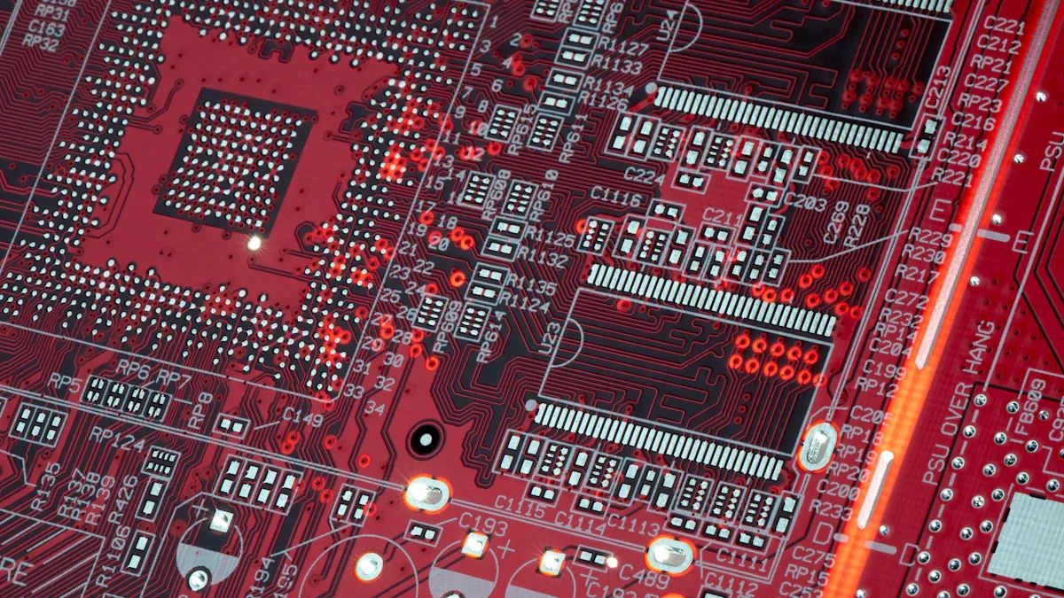
Ignoring Design Rules and Guidelines
Ignoring design rules can lead to significant issues during manufacturing and operation. For example, insufficient annular rings may cause drill breakage, increasing production costs. Misrouted connections can result in crosstalk or circuit failure. Additionally, mismatches between Gerber files and schematic drawings often lead to misplaced components, affecting the functionality of your PCB.
Consequence | Description |
|---|---|
Manufacturing issues | Insufficient annular rings can lead to problems during drilling, causing drill breakage and increased costs. |
Incorrectly placed components | Misplacement of components can lead to errors during assembly, affecting functionality and causing short circuits. |
Signal interference | Signal reflection from stubs can lead to crosstalk and other signal-integrity issues. |
Overheating risk | Excessive current flow due to high copper weight can cause overheating. |
To avoid these problems, always follow industry-standard guidelines. Double-check your design for compliance with manufacturing tolerances and ensure proper trace spacing. This approach minimizes production delays and ensures your circuit performs reliably.
Poor Component Placement on the PCB
Improper component placement can complicate assembly and reduce the performance of your PCB. For instance, mixing lead-free and non-lead-free components may cause soldering issues. Placing through-hole components on both sides of the board can also increase manufacturing complexity.
Follow these best practices to ensure proper placement:
Place through-hole components on the top side of the board.
Keep surface-mount devices (SMDs) on the same side whenever possible.
Arrange connectors along the board’s edge, followed by main chips and auxiliary components.
Orient similar components in the same direction to simplify routing and soldering.
Distribute weight evenly by strategically placing large components.
Additionally, group components with similar voltage and current levels together. This reduces interference and improves circuit performance. By following these steps, you can create a well-organized layout that simplifies manufacturing and enhances reliability.
Overlooking Signal Integrity Issues
Signal integrity issues can degrade the performance of your circuit. Problems like crosstalk and switching noise often arise from poor trace routing. For example, placing traces too close together increases interference, while stub traces can cause signal reflections.
To address these issues, increase the separation between adjacent signal traces. Use differential signaling and tightly coupled differential pairs to minimize noise. Placing power and ground planes close together also helps reduce signal degradation. Additionally, decoupling capacitors can decrease ground bounce and improve overall stability.
Avoiding signal integrity problems ensures your PCB operates efficiently. By implementing these strategies, you can maintain high-quality signals and prevent performance issues in your design.
Failing to Test and Validate the PCB Design
Skipping the testing and validation phase can lead to costly mistakes and unreliable PCBs. Testing ensures your design functions as intended and meets performance standards. Without it, you risk producing boards with defects that could compromise your entire project.
To validate your PCB design effectively, follow these steps:
Review the schematics. Check for errors or inconsistencies in your circuit connections. This step helps you catch mistakes early.
Conduct electrical testing. Perform continuity checks to verify connections and analyze signal integrity to ensure stable performance.
Use simulation software. Simulate your design to predict how it will behave under real-world conditions. This process highlights potential issues before fabrication.
Test the prototype. After manufacturing, inspect the board for physical defects and measure electrical parameters to confirm functionality.
Document findings. Record any problems you identify and propose solutions. This documentation streamlines future iterations.
💡 Tip: Testing early and often saves time and money. It also prevents defective products from reaching customers.
Neglecting these steps can result in poor signal quality, overheating, or even complete circuit failure. For example, untested designs may suffer from short circuits due to incorrect trace routing. Signal distortion can also occur if you overlook impedance mismatches. These issues not only affect performance but may also damage components.
By prioritizing testing and validation, you ensure your PCB meets design goals and operates reliably. This process builds confidence in your final product and reduces the risk of costly rework. Always remember, a well-tested PCB is the foundation of a successful electronic device.
Best Practices for Successful PCB Design
Start with a Clear and Detailed Plan
A successful printed circuit board begins with a well-thought-out plan. This step ensures your design process stays organized and efficient. Start by defining the specifications of your PCB. This includes identifying the circuit’s purpose, power requirements, and physical constraints. A clear specification aligns all stakeholders and sets unified design goals.
Next, create a conceptual blueprint. This serves as a bridge between planning and implementation, helping you visualize the layout and functionality of your circuit board. Once the blueprint is ready, develop detailed schematics. These diagrams represent the electrical interconnections and ensure accurate design representation. By following these steps, you can avoid confusion and costly mistakes later in the process.
💡 Tip: A detailed plan saves time and simplifies troubleshooting during the design phase.
Follow Industry-Standard Design Guidelines
Adhering to industry standards ensures your PCB meets quality and performance expectations. Start by defining board design rules. These rules help you achieve high fabrication and assembly yields. For example, via sizes should accommodate the required current, and solder mask clearances must allow proper solderability. Annular ring sizes also need to be sufficient for reliable electrical connections.
Strategic component placement is another key guideline. Group components by type to minimize routing complexity and place power and ground planes in optimal locations within the PCB stack-up. Additionally, mechanical constraints, such as connector locations, should guide your layout decisions.
Standards like IPC-A-600 and IPC-6012 provide essential criteria for PCB quality and durability. Following these guidelines ensures your circuit board performs reliably and meets industry expectations.
Optimize Component Placement and Routing
Proper component placement and routing are critical for a functional PCB. Begin by grouping power conditioning components together. This minimizes signal interference and improves circuit performance. Place high-speed signal components close to each other to keep signal paths short. Avoid mixing analog and digital circuits to prevent crosstalk.
During routing, implement continuous power planes unless a split is necessary. Ensure routing channels are adequate for all components, and auto-group repetitive design blocks to enhance efficiency. Test points should also be placed conveniently to simplify debugging and testing. Performing frequent Design Rule Checks (DRC) during the design process helps catch errors early, saving time and effort.
By optimizing placement and routing, you can create a circuit board that is both reliable and easy to manufacture.
Test, Iterate, and Collaborate for Better Results
Testing and iteration are essential steps in creating a reliable PCB. By testing your design at every stage, you can identify and fix issues before they escalate. Start by reviewing your schematic and layout for errors. Use simulation tools to predict how your circuit will behave under real-world conditions. These steps help you catch potential problems early, saving time and resources.
Iteration allows you to refine your PCB design. After testing, make adjustments based on the results. For example, if you notice signal interference, you can reroute traces or adjust component placement. Each iteration brings your design closer to perfection. This process ensures your circuit meets performance standards and operates reliably.
Collaboration enhances the testing and iteration process. When you work with a team, you gain access to diverse perspectives and expertise. Modern tools make collaboration easier than ever. Teams can access design files from anywhere, enabling real-time updates and seamless communication. Centralized data storage ensures everyone works with the latest information, reducing inconsistencies. The table below highlights the benefits of collaboration in PCB projects:
Benefit | Description |
|---|---|
Accessibility and Collaboration | Teams can access design files from anywhere, enabling seamless collaboration and real-time updates. |
Real-Time Communication | Tools like chat and video conferencing facilitate quick discussions and decision-making, speeding up the iteration process. |
Centralized Data Storage | A single repository for design files ensures all members have the latest information, reducing inconsistencies. |
Streamlined Workflows | Automation of repetitive tasks and notifications helps maintain consistent processes and reduces iteration time. |
By combining testing, iteration, and collaboration, you can create a PCB that meets your goals. This approach not only improves the quality of your circuit but also streamlines the entire design process.
Understanding PCB design basics is essential for creating reliable and efficient electronic devices. By mastering the workflow, you can confidently select components, create schematics, and prepare your PCB for manufacturing. Following design rules and synchronizing schematics with layouts ensures your designs are both functional and manufacturable. Tools like KiCad, EAGLE, and Altium Designer simplify schematic capture and layout creation, while prototyping and testing validate your design before production.
To succeed, focus on clear planning, proper component placement, and thorough testing. Apply these principles to your projects, and you’ll build high-quality PCBs that meet your goals. Start small, iterate often, and let your creativity shine through your designs.
FAQ
What is the difference between a schematic and a PCB layout?
A schematic is a diagram showing how components connect electrically. It uses symbols to represent parts and their connections. A PCB layout, on the other hand, is the physical design of the board, showing where components and traces are placed.
How do you choose the right PCB design software?
Choose software based on your project needs. For simple designs, free tools like KiCad work well. For complex projects, professional tools like Altium Designer offer advanced features. Evaluate usability, libraries, and compatibility before deciding.
Why is testing a PCB prototype important?
Testing ensures your PCB functions as intended. It helps you identify design flaws, verify performance, and avoid costly errors during production. Skipping this step can lead to unreliable devices or complete failure.
What are vias in PCB design?
Vias are small holes that connect different layers of a PCB. They allow signals or power to pass between layers. Types include through-hole, blind, and buried vias, each serving specific design purposes.
Can you reuse PCB designs for new projects?
Yes, you can reuse designs by saving templates or modules. This approach saves time and ensures consistency. However, always review and adapt the design to meet the requirements of your new project.