Smart watch PCBs are the essential components of every smartwatch. They enable compact designs while maintaining functionality. Understanding how these smart watch PCBs are manufactured and replicated can inspire innovative concepts. However, challenges arise during these processes. Ethical dilemmas and technical issues frequently occur, particularly in the realm of replication. Addressing these challenges requires a blend of creativity and diligence. Whether you are studying PCB design or producing them, your expertise can contribute to the advancement of wearable technology.
Key Takeaways
Know what your smartwatch PCB needs to do. Its size, battery, and features are key for a good design.
Pick the best design software to make PCB work easier. Tools with auto-routing and error checks save time and help accuracy.
Testing is very important. Try out your design and make samples to find problems before making many, ensuring it works well.
Choose strong and flexible materials. Options like FR4 and PTFE fit different needs and affect cost and performance.
Follow copyright rules when copying PCBs. Always ask permission and credit the original creators to support new ideas.
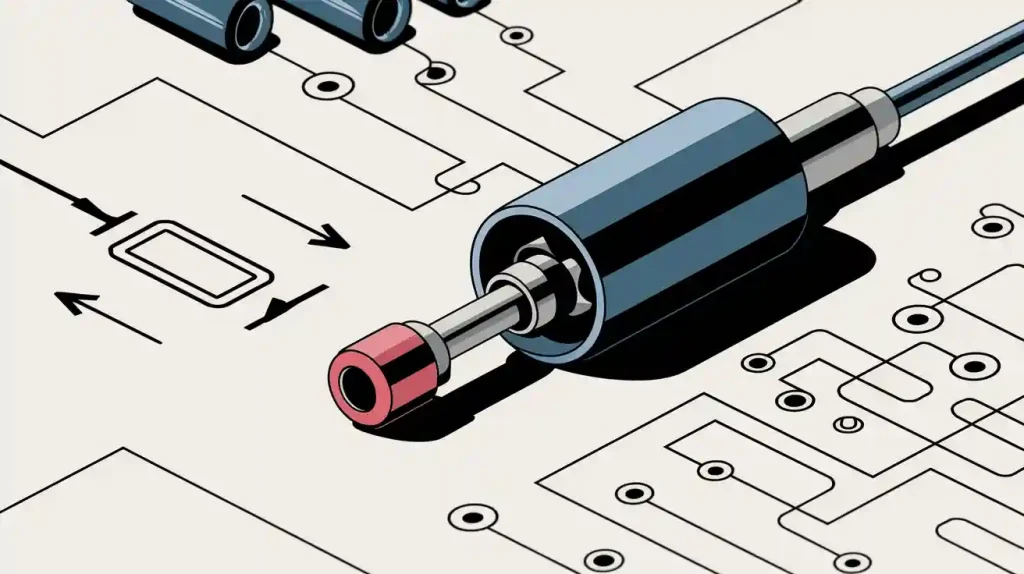
PCB Design for Smart Watches
Understanding functional requirements and specifications
Before making a smartwatch PCB, know what it needs to do. Think about its size, battery use, and features like Bluetooth or Wi-Fi. For example, a fitness watch might need heart rate and step sensors. Knowing these needs helps you design a PCB that fits everything without wasting space.
The PCB market is growing fast because of new technology. By 2025, it could be worth $76 billion. This growth is due to the demand for small, useful PCBs in gadgets like smartwatches. It’s important to design PCBs that match current trends and work well.
Selecting design software and tools
Picking the right tools makes PCB design easier and faster. Modern software has features that save time and improve accuracy. For example, auto-routing tools can quickly connect circuits. Multi-board tools help with designs that use more than one board. 3D checking tools make sure all parts fit together properly.
Here’s a simple table of helpful PCB software features:
Feature | Benefit |
|---|---|
Auto-routing | Quickly connects circuits, saving time. |
Multi-board design | Makes complex designs easier to handle. |
Error checking | Finds mistakes early, so you don’t redo work. |
Supply chain tools | Helps you find parts and replacements. |
Using these tools makes designing smartwatch PCBs faster and more reliable.
Creating schematics and layouts
After choosing your tools, start with a schematic. This is like a map showing how parts connect. Add details like the date, page size, and what the circuit does. Notes and comments can make it easier to understand.
Next, work on the layout. Fit all the parts together while keeping it small. For example, a custom Arduino smartwatch PCB removed extra parts and combined important ones. This saved space and made it work better. Using multi-layer PCBs can also help fit more circuits in less space.
By following these steps, you can design a smartwatch PCB that works well and looks good.
Compact design considerations for smart watch PCBs
When making a smartwatch PCB, keeping it small is key. All parts must fit in a tiny space but still work well. A smart, compact design boosts performance and makes the watch better to use.
Making things smaller has many advantages. Smaller antennas can improve signals by up to 50%. Flexible printed circuit boards (FPCBs) are also helpful. They make the PCB about 30% lighter and handle higher frequencies. This is perfect for smartwatches, which need to be light and work fast.
To save space, use multi-layer PCBs. These stack circuits on top of each other. Integrated circuits (ICs) are also useful. They combine many functions into one chip, reducing parts. Placing components carefully avoids signal problems and spreads power efficiently.
Testing and validating the design
After designing, testing and checking are very important. These steps find and fix problems before making the PCB. Start by using design software to run tests. Simulations check how the circuit works without needing a real model.
If the simulations go well, make a prototype PCB. Test it in real life for issues like overheating or weak signals. Also, check if it works with other smartwatch parts like sensors and batteries.
Testing makes sure the PCB does what it should. It also checks if it follows industry rules. Careful testing and checking help avoid big mistakes and create a great product.
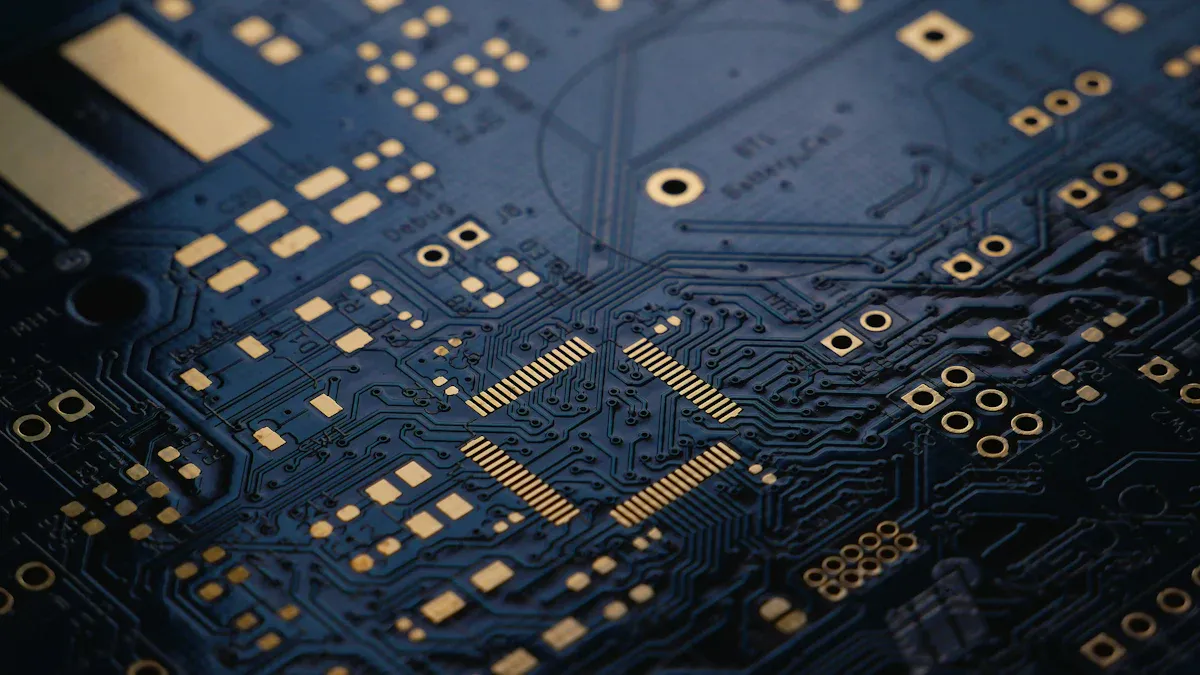
Manufacturing Smart Watch PCBs
Material selection for durability and flexibility
Picking the right materials is very important for smart watch PCBs. The materials must handle small sizes and work well under pressure. They also need to be strong and flexible. Common choices include FR4, PTFE, and metal core. Each has special benefits for different uses.
Material | Properties | Advantages |
|---|---|---|
FR4 | Reliable, fast signals, dielectric constant of 4.5 | Affordable, great for high-frequency tasks |
PTFE | High-speed use, strong, resists fire | Stable in heat, perfect for smartwatches |
Metal Core | Controls heat, manages temperature well | Durable, lightweight, and cost-friendly |
Think about your PCB’s needs when picking materials. For fast data transfer, PTFE works best. If heat control is key, metal core materials are a smart pick.
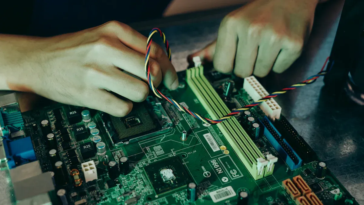
Prototyping and fabrication techniques
Prototyping helps test and improve smart watch PCB designs. It’s a key step before making many copies. Many companies use 3D printing for quick prototypes. This method helps test ideas like button spots or water resistance. For example, a startup used 3D printing to fix smartwatch case flaws early.
After finalizing the prototype, CNC machining is often used. CNC machining ensures accuracy and strength. It’s a top choice for making final prototypes. Using both methods balances speed and precision during development.
Quality control during production
Keeping high quality during production is very important. Quality control includes several checks to find and fix problems early.
Inspection Stage | What Happens | What Is Checked |
|---|---|---|
Initial inspection | Inspectors compare the PCB to design plans. | Size, layout, and part placement |
Component inspection | Inspectors check all parts are in the right place. | Placement of resistors, capacitors, and other parts |
Soldering inspection | Inspectors look at solder joints. | Smooth joints, no bridges, no weak spots |
Final check | Auditors look for visible problems. | Labels, markings, and overall build |
To keep quality consistent, write down steps, use updated files, and work with trusted suppliers. Listening to customer feedback also helps improve the process. Following these steps ensures you make reliable products that meet industry rules.
Partnering with reliable PCB manufacturers
Picking the right PCB maker is very important. A good manufacturer ensures your designs are accurate and meet standards. Check their skills, tools, and past work before choosing.
Look for manufacturers with experience in small, advanced PCBs. Companies that focus on wearables or custom PCBs are ideal. They often use special methods like multi-layer stacking or flexible PCBs.
Clear communication is key to a good partnership. Share your design needs and goals with them. A good manufacturer will give advice and suggest better ideas. They can also help pick materials for stronger and better PCBs.
Quality checks are also very important. Reliable manufacturers test PCBs for problems and compatibility. Ask about their testing steps and certifications to ensure high standards.
Price matters, but don’t only focus on cost. Cheaper options might lower quality or cause delays. Instead, find a balance between cost and reliability. Many manufacturers let you adjust production sizes as needed.
Building trust with your manufacturer helps in the long run. A reliable partner can assist with future projects and keep you competitive.
Copying and Replicating Smart Watch PCBs
Reverse engineering and its applications
Reverse engineering helps you learn how a smart watch PCB works. By studying the board, you can find its parts and connections. This lets you understand its functions and fix problems. For instance, if a smartwatch breaks, reverse engineering can locate the issue and solve it.
You can also use reverse engineering to make designs better. By examining a PCB, you might find ways to make it smaller or faster. But always follow intellectual property laws and act ethically when doing this.
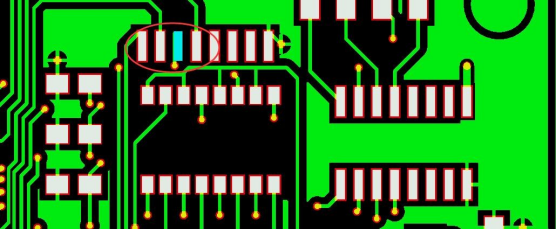
Tools and techniques for PCB replication
Copying a PCB needs special tools and methods. Software like Altium Designer® 24 makes this easier. It helps you copy layouts for repeated circuit parts. This saves time and keeps the design accurate. The software also provides guides to protect the original design’s quality.
Here are some tools and methods for PCB copying:
Schematic capture tools: Help you draw the PCB’s circuit diagram.
PCB layout editors: Let you design how the board looks physically.
Multimeters and oscilloscopes: Test and check if the copied PCB works.
Using these tools well takes practice and care. Always check your work to avoid mistakes.
Ethical and legal considerations in copying
When copying a smart watch PCB, think about ethics and laws. Copying without permission can break intellectual property rules and cause legal trouble. Always ask the original creator before copying their design.
Being ethical means giving credit to the original designers. Avoid stealing ideas or claiming them as your own. Respecting these rules helps create a fair and creative industry. Remember, copying should be for learning or improving, not for stealing ideas.
Intellectual property concerns
When copying a smartwatch PCB, follow intellectual property (IP) laws. These rules protect the creator’s rights and their designs. Breaking these laws can lead to fines or lawsuits.
There are three main types of IP concerns:
Patents: Protect new inventions or methods. Copying patented PCB designs without approval is illegal.
Copyrights: Cover creative works like PCB layouts and schematics. Even reverse-engineered designs may still have copyright protection.
Trademarks: Protect brand names, logos, or symbols. Using trademarked logos on copied PCBs can confuse buyers and break the law.
Tip: Check if a PCB design has patents, copyrights, or trademarks before copying it. This can help you avoid legal problems.
Respect the creator’s hard work and ideas. Copying without credit is unfair and discourages innovation. Instead, learn from designs to make better ones.
If copying for learning, you may have more freedom. But using designs for profit without permission is wrong. Always ask the creator if you’re unsure.
By respecting IP laws, you support a fair tech industry. Following these rules keeps you safe legally and builds trust in your work.
Challenges and Troubleshooting in PCB Design and Manufacturing
Fixing design and layout problems
Making a smartwatch PCB can be tricky. Fitting many parts into a small space is hard. This can cause performance issues. Tight spaces may lead to signal problems like interference or data loss. More parts also create more heat, making cooling important.
To solve these problems, use better designs. Switching from a two-layer to a four-layer PCB helps. It gives more space for routing and reduces clutter. For example, using a sandwich design for battery connections avoids soldering stress. It also makes installation easier. Moving parts around can improve soldering and battery fit. These changes fix layout problems and make the PCB work better.
Problem | Solution |
|---|---|
PCB Layers | Changed from 2-layer to 4-layer for better routing. |
Battery Connection | Used sandwich design to reduce soldering stress. |
Part Placement | Adjusted placement for easier soldering and better battery fitting. |
Solving manufacturing problems
Making smartwatch PCBs can have errors. Common problems include bad solder joints, misplaced parts, and heat damage. These issues can make the hardware unreliable and cost more to fix.
To avoid these problems, use strict quality checks. Inspect every step, from design to assembly. Automated optical inspection (AOI) tools can find misplaced parts or soldering mistakes. Test prototypes in real conditions to catch hidden issues. For example, checking motor resistance (about 30 ohms) can improve reliability. Fixing problems early saves time and money while ensuring good quality.
Making sure parts work together
Smartwatch PCBs must work well with sensors, batteries, and screens. Problems happen if the PCB doesn’t match these parts. For instance, a bad connection for a TFT screen can make assembly harder and less durable.
To avoid this, pick the right parts and design carefully. Use cable connectors for screens instead of soldering directly. This makes assembly easier. Increasing pullup resistor resistance in new PCB versions can fix performance issues. Always test the PCB with real parts before mass production. This ensures everything works together and improves the smartwatch’s performance.
Tip: Test your PCB with real parts early to find and fix problems.
Cost-saving tips for making smart watch PCBs
Making smart watch PCBs cheaply helps save money and stay competitive. Using smart methods, you can cut costs but keep good quality. Here are some easy ways to make PCB production cheaper.
First, improve how you make PCBs. Shorter production times save money and boost efficiency. For example, cutting production time by 25% can lower costs a lot. You can do this by organizing tasks better and using machines for repeated jobs.
Next, try to avoid mistakes during production. Fewer mistakes mean less waste and less time fixing errors. Companies that lower mistakes by 15% often do better in the market. Regular checks and advanced tools can help you find and fix problems early.
Using new technology can also save money. Before buying new tools or software, check if they’re worth the cost. For instance, tracking how much equipment is used can improve efficiency by 20%. This ensures you get the best use of your tools.
Eco-friendly methods can save money too. Using green materials and energy-saving techniques can cut costs by 20%. These methods also attract customers who care about the environment.
Here’s a table showing important things to track for saving money:
Metric | What It Means |
|---|---|
Faster Production | Shorter lead times improve efficiency by 25%. |
Fewer Mistakes | Reducing errors by 15% makes production better. |
Better Equipment Use | Tracking usage boosts efficiency by 20%. |
Green Practices | Eco-friendly methods save up to 20% in costs. |
By following these tips, you can make great PCBs without spending too much. Checking these points often keeps your process cheap and effective.
Making, designing, and copying a smartwatch PCB needs many steps. Each step, like picking materials or checking quality, is important. These steps help make a strong and useful product. For example, rigid devices use simple methods, but stretchable ones need special techniques like liquid metal. Here’s a comparison:
Step | Rigid Device | Stretchable Device |
|---|---|---|
1 | Get materials | Get materials |
2 | Make the base | Create stretchable base |
3 | Add components | Use liquid metal |
4 | Put it together | Place parts carefully |
5 | Check for problems | Check for problems |
6 | Dispose or recycle | Recycle or burn |
Being honest and creative is key in PCB work. Always respect others’ ideas and make your own unique designs. Use this knowledge to think of new ideas and get better at your craft. The future of smartwatches depends on your hard work and imagination.
FAQ
1. What does a PCB do in a smartwatch?
The PCB is like the brain of a smartwatch. It links parts like sensors, batteries, and processors. This connection makes everything work together. Without it, the smartwatch won’t work.
2. Can you make a smartwatch PCB without expensive tools?
Yes, you can use free or cheap tools like KiCad or EasyEDA. These tools help you draw circuits and plan layouts. But advanced tools are better for tricky designs.
3. How can you make a PCB smaller?
Use multi-layer PCBs and integrated circuits to save space. These methods stack circuits and combine functions. Placing parts carefully also helps make it compact.
4. Is copying a smartwatch PCB allowed?
Copying for learning is usually okay. But selling or sharing copied designs without permission breaks the law. Always check for patents or copyrights before copying.
5. What materials work best for smartwatch PCBs?
Common materials include FR4, PTFE, and metal core. FR4 is cheap and reliable. PTFE is great for fast tasks. Metal core materials handle heat well and are durable.
Tip: Pick materials based on your smartwatch’s needs, like flexibility or heat control.