Table of Contents
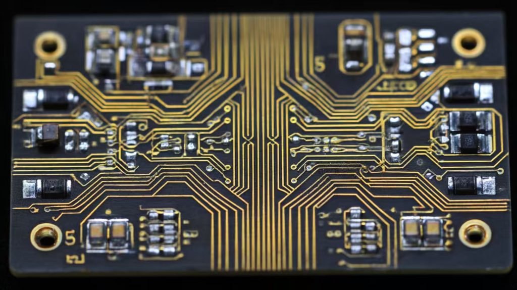
Printed Circuit Board (PCB) copy and reverse engineering play a vital role in modern electronics. PCB copy involves replicating an existing board’s design to create identical functionality. Reverse engineering, on the other hand, dissects a PCB to understand its structure and operation. These methods are essential for solving challenges like replacing obsolete components or troubleshooting complex devices. For instance, engineers reverse engineered a critical PCB for a Florida power company, restoring operations after a shutdown. Globally, PCB reverse engineering has become a cornerstone of innovation, especially in regions like China, where it drives research and development.
Key Takeaways
- PCB copying lets you make copies of circuit boards. This helps replace old parts or keep backups.
- Reverse engineering lets you study and improve circuit designs. It can make them work better and follow rules.
- Using proper tools, like microscopes and software, is important. These tools help make PCB copying and reverse engineering precise.
- Always follow intellectual property laws to stay out of legal trouble.
- These methods save money and make product development faster. This helps products reach the market quickly and encourages new ideas.
What is PCB Copy and Reverse Engineering?
PCB Copy: Definition and Purpose
PCB copy involves duplicating an existing printed circuit board using technical methods. This process ensures the replicated board matches the original in functionality and design. You might use PCB copy to replace outdated components or create backups for critical systems. Unlike reverse engineering, PCB copy focuses on exact duplication rather than analyzing or improving the design. For example, engineers often rely on PCB copy to maintain legacy systems where original designs are unavailable.
Reverse Engineering: Definition and Applications
Reverse engineering dissects a PCB to understand its structure, functionality, and design. Instead of creating an identical copy, you analyze the board to gain insights or make improvements. This method serves several purposes:
- Design validation
- Troubleshooting
- Quality control
- Manufacturing optimization
- Replacing obsolete components
- Gaining insights into competitor products
- Iterative design improvements
For instance, reverse engineering can help you redesign a PCB to comply with environmental regulations like WEEE or RoHS. It also allows you to integrate new technologies into older systems, enhancing their performance.
Key Use Cases
Product Replication
PCB copy is invaluable for replicating products when original designs are lost. You can use it to recreate obsolete devices or ensure compatibility with existing systems. For example, engineers often replicate vintage audio amplifiers by copying their PCBs to replace outdated components.
Troubleshooting and Repairs
Reverse engineering helps you troubleshoot and repair malfunctioning devices. By analyzing the circuit, you can identify faults and replace damaged components. This approach is especially useful for maintaining older systems where documentation is unavailable.
Innovation and Design Enhancements
Reverse engineering fosters innovation by allowing you to improve existing designs. You can integrate emerging technologies, enhance functionalities, or reduce manufacturing costs. For example, companies often reverse engineer competitors’ products to uncover design strategies, such as improving battery life in smartphones.
Tip: Whether you’re replicating a PCB or reverse engineering one, always ensure you comply with intellectual property laws to avoid legal issues.
Step-by-Step Process for PCB Copy and Reverse Engineering
Tools and Equipment
Essential Hardware Tools
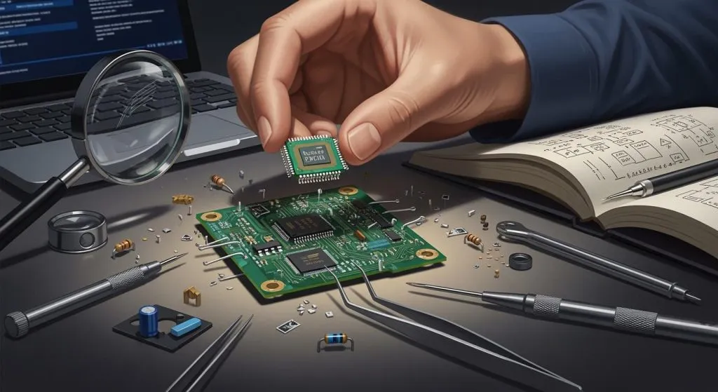
To successfully perform PCB copy or reverse engineering, you need the right tools. Start with optical inspection tools like high-resolution microscopes and cameras. These help you examine the PCB layout in detail. X-ray inspection equipment is another essential tool. It allows you to analyze hidden layers and vias without damaging the board. Electrical testing equipment, such as multimeters and oscilloscopes, is crucial for checking the functionality of components. These tools ensure you can identify faults and verify performance effectively.
Software Tools for PCB Design
Software tools play a vital role in both PCB copy and reverse engineering. Programs like Altium Designer and KiCad help you recreate schematics and layouts. These tools simplify the process of tracing copper paths and generating Gerber files for fabrication. They also reduce errors, making the process more efficient and accurate.
PCB Copy Process
Inspecting and Documenting the PCB
Begin by carefully inspecting the PCB. Record all visible components, their placements, and connections. This documentation forms the foundation for the entire process.
Layer Scanning and Component Removal
Next, desolder the components and clean the board. Use a scanner to capture high-resolution images of each PCB layer. This step ensures you can accurately trace the layout later.
Recreating the Schematic and Layout
Import the scanned images into PCB design software. Trace the copper paths and recreate the schematic. Once complete, export the design as Gerber files for manufacturing. Finally, assemble and test the new board to ensure it matches the original.
PCB Reverse Engineering Process
Identifying Components and Traces
Reverse engineering starts with identifying all components and their connections. Use tools like microscopes and multimeters to map out the circuit.
Circuit Analysis and Evaluation
Analyze the circuit to understand its functionality. This step helps you identify areas for improvement or troubleshoot issues.
Reconstructing the PCB Design
Rebuild the PCB layout using design software. Create a schematic, generate a bill of materials (BOM), and prepare the design for fabrication. This process ensures you can replicate or enhance the original design.
Note: Both processes require precision and attention to detail. Using reliable tools and software ensures accuracy and reduces the risk of errors.
Benefits and Challenges of PCB Copy and Reverse Engineering

Benefits
Cost Efficiency
PCB copy and reverse engineering can save you significant costs. Instead of designing a circuit board from scratch, you can replicate or analyze an existing design. This approach reduces research and development expenses. For example, copying a PCB allows you to maintain legacy systems without investing in entirely new designs. By reusing proven layouts, you also minimize the risk of costly design errors.
Accelerated Prototyping
These methods speed up the prototyping process. By copying and improving existing designs, you can bring products to market faster. For instance, PCB copy shortens the development cycle, enabling quicker iterations. The table below highlights some key benefits:
| Benefit | Description |
|---|---|
| Accelerate product development | PCB copyboards shorten the development cycle by copying and improving existing designs, allowing for quicker market entry. |
| Reduce R&D costs | PCB copying minimizes the high costs associated with designing and manufacturing from scratch, saving resources. |
Learning Opportunities
Reverse engineering offers valuable learning experiences. You gain insights into circuit design and manufacturing processes. By analyzing high-quality products, you can improve your own design skills. The table below outlines some of the learning opportunities:
| Learning Opportunity | Description |
|---|---|
| Knowledge and Skills | Participants learn to de-process, analyze, and recreate design files of electronic devices. |
| Techniques and Tools | The course covers techniques and tools required for PCB reverse engineering. |
| Practical Hands-on Exercises | Participants engage in hands-on exercises to gain expertise in reverse engineering methodologies. |
| Real-world Examples | The course includes real-world examples to enhance understanding of PCB analysis. |
You can also explore manufacturing techniques and refine your layout strategies by studying existing PCBs.
Challenges
Technical Complexity
Modern PCBs often feature dense layouts and multiple layers, making reverse engineering challenging. Internal layers and embedded components add to the complexity. To overcome these obstacles, you can use advanced tools like X-ray inspection and specialized software. Breaking the process into smaller steps, such as schematic generation and BOM creation, also helps manage the workload.
Time and Resource Demands
PCB copy and reverse engineering require significant time and resources. You need to invest in high-quality tools and dedicate time to tasks like component identification and circuit analysis. Thorough preparation, including cleaning the PCB and gathering the right equipment, can streamline the process. Effective planning ensures you balance thoroughness with project constraints.
Risk of Errors
Errors in reverse-engineered designs can lead to failures. Misidentifying components or missing connections can compromise the final product. To reduce these risks, you should implement quality control measures and use simulation tools. Verifying your work at each stage ensures accuracy and reliability.
Tip: Always follow legal and ethical guidelines to avoid potential issues during PCB copy or reverse engineering projects.
Legal and Ethical Considerations
Intellectual Property and Compliance
Copyright and Patent Issues
When working with PCB reverse engineering, you must navigate intellectual property laws carefully. These laws protect original designs and innovations, ensuring fair competition. Reverse engineering can help identify potential patent infringements or trade secret violations. For example:
- Companies often analyze PCB designs to detect unauthorized copying.
- Protecting your innovations is essential to maintaining a competitive edge.
- Unlicensed reverse engineering may infringe on copyrights, patents, or trade secrets.
You should always consult legal experts to understand the specific laws in your jurisdiction. In many countries, reverse engineering is legal for purposes like repair or analysis. However, using it for unauthorized cloning or counterfeiting is illegal.
Avoiding Legal Infringements
To avoid legal pitfalls, you must approach PCB reverse engineering responsibly. Follow these steps:
- Respect intellectual property rights by adhering to relevant laws.
- Consult legal counsel to ensure compliance with regulations.
- Avoid using reverse engineering for unethical purposes, such as counterfeiting.
By taking these precautions, you can protect yourself from legal action while fostering innovation.
Ethical Practices
Responsible Use of Reverse Engineering
Ethical dilemmas often arise in PCB reverse engineering. For instance, misrepresenting a product as another company’s design is unethical.
This is unethical. Company P is representing itself as Company C to the computer system performing maintenance. If problems were to develop with the Company P drive, it would be probable that the Computer System Support at the Customer Company would telephone the Company C for help or make a complaint. In many cases the drives are not visible to the user, so if the computer tells the user the drive is from Company C then the user will believe it. In my opinion, Company P is representing itself as Company C — that is clearly unethical.
To avoid such issues, you should:
- Conduct reverse engineering within legal and ethical boundaries.
- Consult legal experts to ensure compliance with applicable laws.
- Respect the intellectual property rights of others.
Promoting Innovation within Legal Boundaries
Reverse engineering can drive innovation when done ethically. Learning from competitors is acceptable, but outright copying is dishonest. You must evaluate legal and moral standards to ensure compliance.
- Collaborate with original equipment manufacturers (OEMs) to access design information legally.
- Use systematic approaches and advanced techniques to overcome challenges.
- Focus on improving your designs rather than replicating others.
By adhering to these principles, you can promote innovation while maintaining honesty and integrity. This approach not only ensures compliance but also fosters a fair competitive environment.
Best Practices for PCB Copy and Reverse Engineering
Preparation and Research
Understanding Legal Requirements
Before starting a PCB copy or reverse engineering project, you must understand the legal framework. Intellectual property laws protect original designs, so you need to ensure compliance. Consult legal experts to clarify whether your project aligns with copyright and patent regulations. This step helps you avoid potential legal disputes and ensures ethical practices.
Gathering Necessary Tools and Resources
Thorough preparation is essential for success. Start by collecting the right tools and resources. Use high-resolution microscopes and cameras for optical inspection. X-ray equipment reveals hidden layers and vias without damaging the board. Electrical testing tools like multimeters and oscilloscopes help you measure component functionality. Follow these steps to prepare effectively:
- Examine the PCB for high-position components and record their details.
- Scan the board before removing components to create a backup.
- Remove components carefully, starting with resistors and capacitors.
- Clean the PCB surface to ensure clear visibility of details.
- Use software tools to process scanned images and recreate the design.
Tip: Always document your work meticulously. Accurate records make the process smoother and reduce errors.
Ensuring Accuracy
Verifying Component Identification
Accurate component identification is crucial. Use optical and microscopic observation to confirm component types and conditions. X-ray inspection reveals hidden features like embedded components and internal layers. Electrical parameter testing with tools like LCR bridges ensures precise measurements. The table below highlights key methods:
| Method | Description |
|---|---|
| Optical and microscopic observation | Examine components visually to confirm their type and condition. |
| X-ray inspection | Analyze hidden layers and embedded components. |
| Electrical parameter testing | Measure electrical characteristics to verify component values. |
Using Reliable Tools and Software
Reliable tools and software improve accuracy. Use advanced EDA software for schematic generation and layout reconstruction. Verify your work at each stage to ensure consistency. Clean the PCB thoroughly to avoid contamination, and adopt a systematic approach by breaking the process into manageable steps.
Note: High-quality tools and software reduce errors and enhance the reliability of your results.
Maintaining Ethical Standards
Respecting Intellectual Property Rights
Respect for intellectual property is non-negotiable. Conduct reverse engineering within legal boundaries and avoid unauthorized replication. Consult legal counsel to ensure compliance with applicable laws. This approach protects you from legal risks and fosters a fair competitive environment.
Focusing on Learning and Innovation
Use reverse engineering as a tool for learning and innovation. Instead of copying designs, focus on improving them. Collaborate with original manufacturers when possible to access design information legally. This mindset promotes creativity and ensures ethical practices.
Reminder: Ethical reverse engineering drives progress while respecting the rights of others.
PCB copy and reverse engineering play a vital role in modern electronics. These methods help you restore lost design files, upgrade functionality, and replace obsolete components. They also allow you to enhance circuits using advanced, cost-effective components. By applying these techniques, you can validate designs, repair faults, and gain insights into competitor products.
You must approach these practices responsibly. Respect intellectual property and focus on innovation rather than replication. Use this knowledge to create better designs while staying compliant with legal standards. With the right mindset, you can drive progress and contribute to the future of electronics.
FAQ
What is the difference between PCB copy and reverse engineering?
PCB copy replicates an existing board exactly, while reverse engineering analyzes a board to understand its design and functionality. You use PCB copy for duplication and reverse engineering for innovation or troubleshooting.
Is PCB reverse engineering legal?
Yes, it is legal if you follow intellectual property laws. You must avoid unauthorized replication or counterfeiting. Always consult legal experts to ensure compliance with copyright and patent regulations.
What tools do I need for PCB reverse engineering?
You need microscopes, multimeters, and X-ray equipment for inspection. Software like Altium Designer or KiCad helps you recreate schematics and layouts. These tools ensure precision and efficiency.
Can I improve a PCB design through reverse engineering?
Yes, reverse engineering allows you to analyze and enhance existing designs. You can integrate new technologies, optimize layouts, or improve performance. This process fosters innovation and learning.
How do I avoid errors during PCB copy or reverse engineering?
Document every step carefully. Use reliable tools and software to ensure accuracy. Verify your work at each stage, from component identification to schematic recreation. This approach minimizes mistakes and ensures quality results.