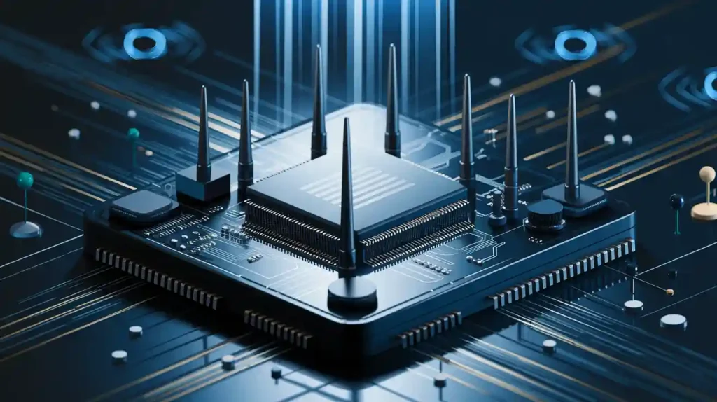
When you begin rf pcb design, you need to care about signal integrity. Good pcb design keeps each signal safe from interference. You have to match impedance for each signal path. Pick the right pcb materials and plan your stack-up well. Put each circuit part in a way that lowers signal loss. Rf pcb design has special problems. Rf signals react to every pcb trace, via, and ground plane. You must keep signal integrity high or the circuit may fail. Learn these basics to make rf circuit boards that work well.
Key basics you need:
Signal integrity management
Impedance matching
Careful pcb stack-up planning
Smart material selection
Best layout practices for every signal and circuit
Remember: Good rf pcb design skills help you avoid mistakes and keep your rf circuit boards working well.
Key Takeaways
Make signal paths short and simple to keep signals strong and stop noise. – Match impedance well so signals do not bounce back or get weak. – Pick special PCB materials like Rogers or Teflon for better high-frequency work. – Plan your PCB layout and stack-up to lower crosstalk and make grounding better. – Do not make common mistakes by checking your design and using simulation tools before you build.
What is RF PCB Design?
RF Circuit Boards Overview
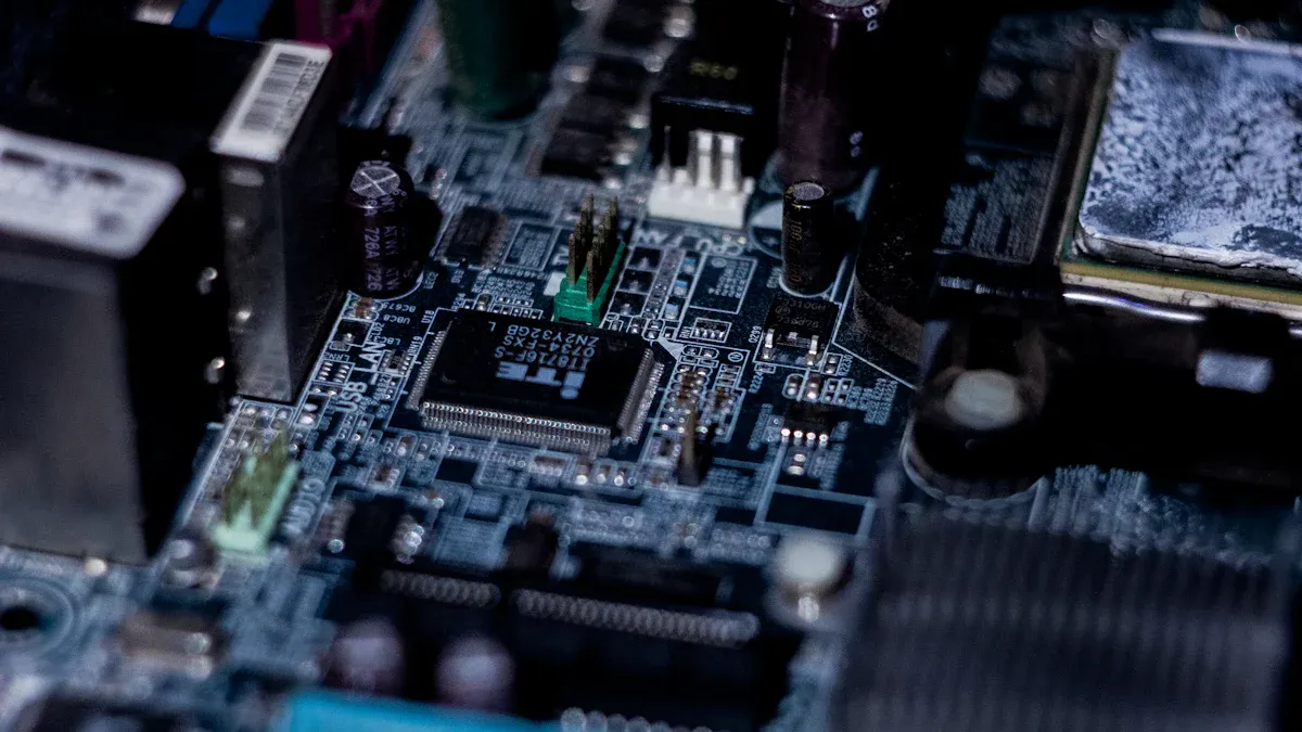
Rf pcb design is used for circuit boards in high-frequency jobs. These boards carry signals that move much faster than normal ones. You can find rf pcb design in things like wireless gadgets, radar, and communication tools. Each board must work well with fast signals and not lose quality.
In rf pcb design, you watch how signals move on the board. You should keep signal paths short and straight. You also need to stop signals from messing with each other. Good pcb design helps you block noise and stop signal loss. Rf circuit boards use special materials because regular ones do not work well for fast signals.
Tip: Always look at the datasheet for each material before you start your pcb design. Picking the right material helps your board work well with fast signals.
Unique Challenges
Rf pcb design has problems you do not see in normal pcb design. Fast signals make every trace, via, and ground plane matter a lot. Even small layout changes can change how signals move. You must plan your design to keep signals strong.
You need to match impedance for each signal path. If you do not, signals can bounce back and cause mistakes. Grounding and shielding are more important in rf pcb design. You must keep signals safe from outside noise and from each other.
Here are some common problems you will see:
Signal loss when signals move fast
Crosstalk between signal traces
Hard to keep impedance right
Heat builds up in crowded areas
Material problems with fast signals
You can fix these problems with careful pcb design and by using good rf circuit board tips. When you learn these basics, you can make boards that work well for all your fast signal needs.
Key Principles
Signal Integrity
You must protect signal integrity in every RF PCB design. High-speed signals move fast across the board. Each signal can lose strength or pick up noise if you do not plan well. Signal integrity issues often come from poor routing, long transmission lines, or bad grounding. You need to keep transmission lines short and direct. This helps each signal stay strong and clear.
High-speed design means you must watch for crosstalk between lines. When two transmission lines run close, signals can jump from one to the other. This causes signal integrity issues and can break your circuit. Use enough space between lines to stop this. Place ground planes under your transmission lines. This gives each signal a safe path and lowers noise.
Tip: Always check your PCB for signal integrity issues before you finish your design. Use simulation tools to see how high-speed signals move on your board.
Impedance Matching
Impedance matching is a key part of RF PCB design. Each transmission line has a set impedance. If you do not match this impedance, signals reflect back. This reflection causes loss and can damage your circuit. You must use controlled impedance for every high-speed signal path.
In high-speed design, you need to know the impedance of your transmission lines. Use the right width and spacing for each line. The PCB stack-up also changes the impedance. Always plan your stack-up before you route lines. Controlled impedance keeps signals from bouncing back and keeps your circuit working.
Impedance matching is more strict in RF PCB design than in standard PCB design. High-frequency signals need tight control. Use tools to check the impedance of your lines. Adjust the width or the PCB material if you see problems. Controlled impedance helps you avoid signal integrity issues and keeps your transmission lines clear.
Note: Impedance matching is not just for RF circuits. You also need it in high-speed board design for digital signals.
Grounding and Shielding
Grounding and shielding protect your signals from outside noise. In RF PCB design, you must use solid ground planes. Place these planes under your transmission lines. This gives each signal a safe return path and lowers noise.
Shielding stops outside signals from getting into your circuit. Use ground fills and guard traces around sensitive lines. This keeps high-speed signals safe from interference. Good grounding and shielding also help with heat control. High-speed design often creates heat in small areas. Solid ground planes help spread this heat.
You must connect all ground points with short, wide lines. This lowers resistance and keeps your circuit stable. In RF PCB design, poor grounding causes signal integrity issues and can break your board. Always check your grounding and shielding before you finish your design.
Remember: Good grounding and shielding are just as important as controlled impedance and signal integrity in every RF PCB design.
Design Steps
Material Selection
You need to pick the right materials first. The material you choose changes how fast signals move. It also affects signal loss and how well your board works. Regular PCB materials are not good for high-speed jobs. You need materials that lose less signal and stay stable at high frequencies. These special materials help keep signals strong and cut down on noise.
When picking materials, always check the datasheet. Look at the dielectric constant and loss tangent numbers. These numbers show how the material handles fast signals. Rogers and Teflon work better than FR-4 for RF circuits. The right material makes your board work better and keeps signals steady.
Tip: Test a small piece of your chosen material before making the whole PCB. This helps you avoid big mistakes.
Stack-Up Planning
Stack-up planning is about how your PCB layers fit together. You need to choose how many layers you want. You also decide where to put ground and power planes. A good stack-up helps with high-speed design and keeps signal loss low. It also helps you match impedance and stop crosstalk.
Put ground planes close to signal layers. This gives each signal a clear path back and lowers noise. Power planes should be next to ground planes to keep voltage steady. The stack-up changes how you route signal lines. Careful planning makes your board work better and easier to build.
Layer | Purpose | Impact on Performance |
|---|---|---|
Top | Signal/Components | Direct signal routing |
2 | Ground Plane | Reduces noise, aids return |
3 | Power Plane | Stabilizes voltage |
Bottom | Signal | Extra routing for signals |
Note: A good stack-up is very important for fast signals and strong RF boards.
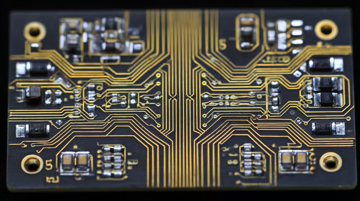
PCB Layout Design
PCB layout design is where you put and connect every part. You should keep signal paths short and straight. Long or twisty traces make signals weak and slow. Put sensitive RF parts far from noisy digital ones. This helps stop interference.
Use wide traces for fast signals. Leave space between lines to stop crosstalk. Put ground fills around important spots. This protects signals and helps your board work better. Always use good layout rules to get the best results.
Keep signal traces straight and short.
Separate RF and digital sections.
Use ground fills and guard traces.
Avoid sharp corners in traces.
Callout: Good PCB layout design is very important for your RF circuit. Take your time and check everything.
Impedance Control
Impedance control is needed in RF PCB design. Each signal line needs a set impedance to keep signals clear. If you do not control impedance, signals bounce back and get weak. Use the right trace width, spacing, and layer stack-up to set impedance.
You need tools to check the impedance of your signal lines. Change the layout if you see problems. Controlled impedance keeps signals strong and your board stable. You must check impedance at every step, not just once.
Alert: Bad impedance control causes signal bounce and weak boards. Always check your numbers.
Component Placement
Component placement affects how well your RF board works. Put RF parts close together to keep signal paths short. Keep sensitive parts away from noisy spots. This helps protect signals and makes your board work better.
Put connectors at the edge of the board for easy use. Keep fast parts near ground planes for a safe return path. Use vias to connect layers but do not use too many. Too many vias can weaken signals.
Group RF parts by what they do.
Put decoupling capacitors close to power pins.
Keep signal lines as straight as you can.
Do not put parts over split ground planes.
Tip: Check your part placement before you finish your layout. Small changes can help your board work better and stop signal problems.
Common Mistakes
Typical Errors
You may face many common mistakes when you start with RF pcb design. These errors can lower the performance of your circuit and cause signal problems. Here are some mistakes you should watch for:
You use the wrong pcb material. This can cause high signal loss and weak performance.
You ignore impedance control. Signals may reflect and lose integrity.
You place signal traces too close together. This leads to crosstalk and noise.
You forget to keep signal paths short. Long traces weaken signals and hurt performance.
You skip proper grounding. Poor grounding lets noise enter your circuit.
You use too many vias. Each via can add loss and change signal path.
You mix digital and rf circuit parts without care. This can cause interference and lower performance.
Tip: Always check your pcb layout for these mistakes before you finish your design.
How to Avoid Them
You can avoid most mistakes with careful planning and good pcb design habits. Here are some ways to keep your rf pcb strong:
Choose the right pcb material for your rf circuit. Check the datasheet for signal loss and stability.
Plan your pcb stack-up early. Place ground planes close to signal layers for better performance.
Keep signal traces short and straight. This helps maintain signal strength and integrity.
Use enough space between signal lines. This reduces crosstalk and keeps signals clean.
Limit the number of vias in your design. Only use them when needed for routing.
Separate rf and digital circuit sections. This stops unwanted noise and keeps performance high.
Test your pcb with simulation tools. Find signal problems before you build the board.
Remember: Careful pcb design helps you avoid costly mistakes and keeps your rf circuit working at top performance.
Tools and Resources
PCB Design Software
You need the right tools to create strong pcb layouts. Good pcb design software helps you plan, draw, and check your boards. Many programs let you see your pcb in 3D and run checks for errors. Some tools also help you control impedance and keep your signal paths clear. You can use these features to make sure your design meets all rf pcb needs.
Here are some popular pcb design software options:
Altium Designer: This tool gives you advanced layout features and strong simulation tools. You can check your pcb for signal issues before you build.
KiCad: This free software works well for beginners. You can draw your pcb and use built-in tools for basic design checks.
Eagle: Many engineers use Eagle for small to medium pcb projects. It has a simple interface and good support for libraries.
Mentor Graphics PADS: This tool offers strong features for complex pcb design. You can use it for high-speed and rf boards.
Tip: Try out a few pcb design programs before you choose one. Pick the one that fits your project and skill level.
Learning Communities
You can learn a lot from other engineers who work on pcb design. Online communities give you a place to ask questions, share tips, and find answers. Many groups post guides, videos, and sample projects. You can join these groups to get help with your own pcb design work.
Some helpful learning communities include:
EEVblog Forum: You can ask about pcb design, rf boards, and signal problems. Many experts share advice here.
Reddit r/PrintedCircuitBoard: This group covers all things pcb. You can find design tips and see real projects.
PCBWay Community: You can read articles, watch videos, and join design contests.
All About Circuits: This site has forums and guides for pcb design and electronics.
Note: Stay active in these communities. You will learn new design tricks and avoid common mistakes.
You have learned the main ideas of RF PCB design. Pay attention to signal integrity and impedance matching. Pick the right materials for your board. Use a smart layout for your design. Try these tips on your first RF project to get better results. Join design groups and learn from people who know more. Keep learning new things as you work on more projects.
🚀 Begin your RF PCB adventure with confidence. Every project teaches you something new and helps you make fewer mistakes.
FAQ
What is the most important factor in RF PCB design?
You must focus on signal integrity. High-frequency signals need clear paths. Good signal integrity keeps your circuit working well. Always check your layout for issues before you finish your design.
Can you use FR-4 material for RF PCBs?
You can use FR-4 for low-frequency RF circuits. For higher frequencies, FR-4 causes signal loss. Choose materials like Rogers or Teflon for better performance at high frequencies.
How do you reduce crosstalk between traces?
Keep enough space between signal traces. Use ground planes under your traces. Place guard traces if needed. These steps help you lower crosstalk and keep signals clean.
Why does impedance matching matter in RF PCB design?
Impedance matching stops signal reflections. If you match impedance, your signals stay strong and clear. Poor matching causes signal loss and weakens your circuit.