You want your RF PCB Design to work very well. To do this, you must keep your signals safe from noise and interference. Signal integrity and EMI control help your circuits stay stable at high frequencies. > Spend time planning your layout and where you put parts. These steps help you stop common mistakes and make your mixed-signal and wireless projects better.
Key Takeaways
Make traces short and straight. This helps signals stay strong and clear. It also lowers noise.
Keep analog and digital parts apart on your PCB. This stops interference and makes things work better.
Use solid ground planes and good shielding. This blocks unwanted noise and controls EMI.
Pick PCB materials with low dielectric loss, like Rogers or PTFE. These are good for high-frequency projects.
Test your design early with software and prototypes. This helps you find and fix problems before making the final boards.
Why RF PCB Design Matters
Signal Integrity
You want your signals to move across the board without problems. Signal integrity means signals keep their shape and power as they go. In RF PCB Design, high-frequency signals can lose quality quickly. You might see things like signal reflections, ringing, or crosstalk. These problems can make your wireless project not work right.
To keep signal integrity strong, you should:
Use short, straight traces for high-frequency signals.
Match the impedance of traces to the source and load.
Put parts close together to make paths shorter.
Do not use sharp corners in your traces.
Tip: Always look at your layout for long or looping traces. These can act like antennas and bring in noise.
When you care about signal integrity, your mixed-signal circuits work better. You will have fewer mistakes and your wireless project will be more reliable.
EMI Challenges
Electromagnetic interference (EMI) can mess up your project. EMI happens when unwanted signals move from one part of the board to another. In mixed-signal designs, digital and analog parts can bother each other. Wireless circuits are even more sensitive to EMI.
You can stop EMI by:
Keeping analog and digital areas apart on your PCB.
Using ground planes to block noise.
Adding shielding to parts that need it.
Keeping fast traces away from noisy parts.
Note: Good grounding helps control EMI. Try to connect all grounds at one spot if you can.
You need to think about EMI from the start. If you do not, you might see random problems or weak wireless range. Careful RF PCB Design helps you stop these issues and make strong, high-performance boards.
Material Selection
Substrate Choice
You need to pick the right base material for your PCB. The substrate acts as the foundation for all your circuits. Most basic boards use FR-4, which works well for many digital projects. However, high-frequency signals need special care. FR-4 can cause signal loss at high frequencies. You should look at materials like Rogers, Teflon (PTFE), or ceramics for better performance. These materials help your signals stay strong and clear.
When you choose a substrate, think about:
The frequency range of your project
The cost of the material
How easy it is to make the board
The size and shape of your PCB
Tip: If you work with wireless or mixed-signal designs, always check the datasheet for the substrate. Some materials handle heat and moisture better than others.
Dielectric Properties
The dielectric constant (Dk) tells you how well a material stores electrical energy. A lower Dk means your signals move faster and lose less power. You want a stable Dk across the frequencies you use. If the Dk changes a lot, your signals can slow down or lose shape.
Loss tangent (Df) is another key property. It shows how much energy the material turns into heat. A low Df means less signal loss. For high-frequency work, always pick a material with a low Df.
Here is a quick comparison:
Material | Dielectric Constant (Dk) | Loss Tangent (Df) |
|---|---|---|
FR-4 | 4.2 – 4.7 | 0.018 |
Rogers | 3.38 | 0.0027 |
PTFE | 2.1 | 0.0002 |
Note: You should match your material’s properties to your project’s needs. This helps you get the best performance and reliability.
Layer Stack-Up & Impedance
Stack-Up Strategies
You need a good layer stack-up to keep your signals clean and strong. The stack-up is the order of copper and insulating layers in your PCB. A smart stack-up helps you control signal paths and reduce noise. You can use more layers to separate signals and power. This makes your board work better at high frequencies.
Here are some common stack-up strategies:
2-layer boards: Use for simple designs. Place signals on the top and ground on the bottom.
4-layer boards: Use for better performance. Place signals on the outer layers. Put ground and power in the middle.
6-layer or more: Use for complex or high-speed designs. Add extra ground and power planes for more isolation.
Tip: Always keep high-frequency signals close to a ground plane. This helps stop noise and keeps impedance steady.
A good stack-up also helps you control impedance. Impedance is the resistance to signal flow. If you match impedance, your signals stay strong and do not reflect back. You can use online calculators or PCB design tools to set the right trace width and spacing.
Reference Planes
Reference planes are large areas of copper that act as a steady voltage point. You use them for ground or power. Reference planes help your signals return to their source. They also block noise and lower EMI.
You should:
Place a solid ground plane under high-speed or RF traces.
Avoid splitting ground planes. This can cause signal loops and noise.
Keep signal layers close to reference planes in the stack-up.
Layer | Use | Benefit |
|---|---|---|
Top | Signal | Easy part placement |
2 | Ground | Good signal return path |
3 | Power | Stable voltage |
Bottom | Signal | Extra routing space |
Note: A strong reference plane makes your board more reliable and easier to debug.
Component Placement
Analog and Digital Isolation
You should keep analog and digital parts apart. Analog signals can pick up noise easily. Digital circuits make quick, sharp signals. These signals can cause problems for analog parts. If you mix them, your board might not work right.
Put analog parts in one spot. Put digital parts in a different spot. Draw a clear line between these two areas. Try to use separate ground planes if you can. If you cannot, connect the grounds at just one point. This helps stop noise from moving between the two sections.
Tip: Put analog traces on one layer and digital traces on another. This helps lower the chance of crosstalk.
You can also use shielding or guard traces. These give extra protection to analog signals that are sensitive.
Compact Layout
A compact layout helps your board work better. Short traces mean less noise and less signal loss. Put parts that work together close to each other. For example, keep decoupling capacitors near power pins.
Here are some steps for a compact layout:
Group parts by what they do.
Keep high-frequency parts close to connectors or antennas.
Do not use long, winding traces.
Place parts so signal paths are straight.
Good Practice | Why It Helps |
|---|---|
Short traces | Less signal loss |
Grouped components | Easier routing |
Direct signal paths | Better performance |
Note: A compact layout also makes your board easier to test and fix.
If you place parts carefully, your board will be stable and reliable. You will have fewer problems with noise and interference.
RF PCB Design Layout

Trace Routing
You need to be careful when routing high-frequency traces. Short and direct traces help signals stay strong. Long traces can act like antennas and pick up noise. Try not to use sharp corners. Use smooth, gentle bends instead. This helps your signal not lose power or bounce back.
Keep traces on the same layer if you can. If you must change layers, do not use too many vias. Each via adds a little inductance. Too many vias can make your signal weaker.
Tip: Put high-frequency traces over a solid ground plane. This gives signals a clear path back and lowers noise.
Here are some good ways to route traces:
Make traces as short as you can.
Use straight paths for important signals.
Do not use 90-degree angles; use 45-degree bends.
Put traces over solid reference planes.
Keep high-frequency and low-frequency traces apart.
A neat routing plan helps stop signal loss and noise. Your mixed-signal and wireless projects will work better.
Signal Line Isolation
You need to keep sensitive signal lines away from noisy ones. Group your PCB into blocks that do different jobs. Put analog, digital, and RF parts in their own areas. This keeps signals from mixing with the wrong group.
Use ground planes or guard traces between different signals. These act like walls and block noise. You can also use shielding cans for very sensitive parts.
Here is a simple table to show ways to keep signals apart:
Technique | How It Helps |
|---|---|
Functional blocks | Cuts down on crosstalk |
Guard traces | Protects sensitive signals |
Ground planes | Blocks out noise |
Shielding cans | Stops outside EMI |
Note: Always look at your layout for places where signals cross. Fix these spots early so you do not have problems later.
You should also keep input and output lines apart. This stops feedback and keeps signals clean. Careful isolation makes your RF PCB Design work better and easier to fix.
Signal Integrity & EMI
Shielding
You want to keep your signals safe from outside noise. Shielding helps you block unwanted signals that can cause problems in your circuit. You can use metal shields, also called cans, to cover sensitive parts of your board. These shields act like walls that stop electromagnetic waves from reaching your important signals.
You can also use ground planes as shields. When you place a ground plane under your traces, you give signals a safe path and block noise from below. Sometimes, you need to use both metal shields and ground planes for the best results.
Here are some ways you can use shielding in your RF PCB Design:
Place metal cans over RF chips or sensitive analog parts.
Use ground planes under high-frequency traces.
Add guard traces next to important signal lines.
Keep shielded areas closed as much as possible.
Tip: Make sure your shield connects to ground at several points. This helps the shield work better and keeps noise out.
A good shield can make your board more reliable. You will see fewer problems with interference and your wireless signals will stay strong.
Grounding
Grounding gives your signals a safe path to return. Good grounding helps you control noise and stop unwanted signals from spreading. You want to use a solid ground plane in your board. This plane acts like a big sheet of copper that collects stray signals and sends them away.
You should connect all your parts to the ground plane with short, wide traces. Thin or long ground traces can act like antennas and bring in noise. Try to keep your ground plane unbroken. If you split the ground plane, you can create loops that pick up noise.
Here is a table to help you remember good grounding practices:
Practice | Why It Matters |
|---|---|
Use a solid ground plane | Stops noise and lowers EMI |
Short, wide ground traces | Gives signals a safe return path |
Connect shields to ground | Improves shielding |
Avoid split ground planes | Prevents ground loops |
Note: In mixed-signal designs, connect analog and digital grounds at one point. This keeps noise from moving between sections.
When you follow these grounding steps, you help your board work better at high frequencies. Your signals stay clean and your project becomes more stable.
Simulation & Testing
Design Software
You need to check your PCB design before you build it. Design software helps you do this. Many engineers use tools like Altium Designer, KiCad, or Eagle. These programs let you draw your circuit and layout your board. You can run simulations to see how signals move. You can also check for errors, like broken connections or wrong trace widths.
Simulation tools help you find problems early. You can test signal paths, impedance, and crosstalk. Some software lets you see how electromagnetic interference might affect your board. You can change your design and test again until you get good results.
Tip: Always use the design rule check (DRC) in your software. This tool finds mistakes that are hard to see.
Here is a table of popular design software and what they offer:
Software | Key Feature | Simulation Support |
|---|---|---|
Altium Designer | Advanced layout | Yes |
KiCad | Free, open source | Yes |
Eagle | Easy to use | Limited |
Prototyping
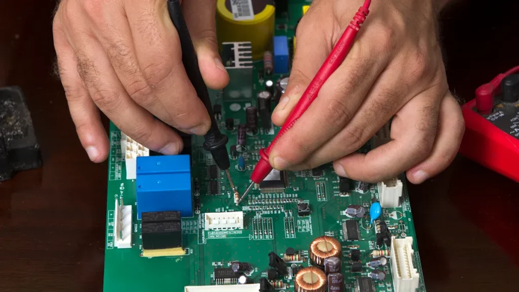
After you finish your design, you need to build a prototype. A prototype is a real board you can test. You order the board from a PCB manufacturer. When you get the board, you solder the parts and check if it works.
You should test each part of your board. Use an oscilloscope to look at signals. Check for noise and signal loss. If you find a problem, you can fix your design and make a new prototype.
Test power and ground first.
Check high-frequency signals with care.
Look for heat or strange behavior.
Note: Testing helps you find mistakes before you make many boards. This saves time and money.
Prototyping gives you real results. You learn what works and what needs to change. Careful testing makes your final product strong and reliable.
You can make your mixed-signal and wireless projects better by using these RF PCB Design tips. Keep traces short so signals stay strong. Use solid ground planes to help stop noise. Put analog and digital parts in different places. Test your board with design software and real boards you build.
Check every step before you start building.
Make a checklist and use it for each project.
Want to know more? Try online classes or join RF design forums to learn new skills.
FAQ
What is the best way to separate analog and digital signals on an RF PCB?
You should place analog and digital parts in different areas. Use a clear line between them. Connect their grounds at one point. This helps stop noise from moving between sections.
How do you reduce EMI in wireless PCB designs?
You can use solid ground planes and short traces. Place shielding cans over sensitive parts. Keep high-speed signals away from analog areas. These steps help block unwanted noise.
Why do trace length and shape matter for RF signals?
Short, straight traces keep your signals strong. Long or bent traces can act like antennas. They pick up noise and cause signal loss. Use 45-degree bends instead of sharp corners.
Which PCB materials work best for high-frequency projects?
You should use materials like Rogers or PTFE for high-frequency work. These have low dielectric loss. Your signals stay clear and strong. FR-4 works for lower frequencies but loses more signal at high speeds.
Can you use free PCB design software for RF projects?
Yes, you can use free tools like KiCad. These let you draw circuits and check layouts. Some free tools offer basic simulation. For advanced features, you may need paid software.