RF PCB design is important for making everyday electronics work. Devices like smartphones and medical tools need strong, reliable circuits. The global PCB market was worth $70 billion in 2022. It might grow to $90 billion by 2027 because of new technology. But designing RF circuits is tricky. Problems like signal interference and layout mistakes can happen. These errors cost over $1 billion each year to fix. Learning RF PCB design helps avoid mistakes, improve signals, and make better devices.
Key Takeaways
Learn the basics of RF PCB design, like frequency needs and picking the right materials, to make good circuits.
Try out simulation tools to check designs before building. This helps find and fix problems early.
Place parts close together and use special routing to reduce signal loss and make circuits work better.
Test prototypes often and study results to improve designs. This makes RF circuits reliable and efficient.
Keep up with new tech and talk to others to grow your skills and knowledge in RF PCB design.
Basics of RF PCB Design
Understanding RF PCB Design
Starting with RF PCB design means learning the basics first. RF circuits work in electromagnetic frequencies above sound and below light. These frequencies range from 30KHz to 300GHz, covering AM radio to satellites. Designing them involves several steps:
Define Requirements: Know the frequency, size, cost, and environment needs.
Design Steps:
Pick an antenna type that fits your needs.
Use the frequency to figure out dimensions.
Test the design using EM simulation tools.
Adjust settings to improve performance.
Build a prototype using different methods.
Test it with tools like a VNA and in special rooms.
Make changes based on test results.
Choosing the right PCB material is very important. Low εr materials make circuits more efficient. FR-4 is cheaper but works better for lower frequencies. Trace design matters too. You need to control impedance, calculate width, and match lengths for high-frequency signals.
Key Concepts and Terminologies
You’ll come across important terms in RF PCB design:
Insertion Loss: This shows how much signal power is lost when a device is added.
VSWR (Voltage Standing Wave Ratio): This checks how well RF power moves from the source to the load.
Characteristic Impedance: This is the impedance a transmission line would have if it were endless.
Knowing these terms helps you follow RF design rules and make better circuit boards.
Common Challenges for Beginners
Beginners in RF PCB design face many challenges:
Signal Integrity: Signals must stay strong and clear in high-speed designs.
Grounding Issues: Bad grounding can hurt performance, especially in RF circuits. Good grounding is key.
Impedance Matching: Matching impedance between parts avoids signal loss and improves efficiency.
Managing Analog and Digital Signals: Handling both signal types can be hard. Careful planning helps manage them better.
By learning about these problems, you can prepare to solve them and get better at RF PCB design.
Picking RF PCB Design Software
What to Look for in RF PCB Tools
Choosing software for RF PCB design is very important. Good tools make designing easier and improve how circuits work. Pick software that handles high-frequency signals well. It should also have strong layout features and EM analysis tools. Easy-to-use software helps beginners learn faster. Tools that work with other programs make teamwork smoother. Libraries with RF parts save time during design. Beginners should also think about cost when choosing software.
Here’s a table of key features to check:
Feature/Consideration | Description |
|---|---|
High-frequency signal handling | Needed for RF circuits to keep signals clear and strong. |
Advanced layout capabilities | Helps place parts and route signals to avoid problems. |
Integration with other tools | Makes designing easier and helps teams work together. |
Comprehensive library support | Offers many RF parts to speed up the design process. |
User-friendliness | Simple interfaces make learning and working faster. |
EM analysis capabilities | Finds and fixes problems with signals and interference. |
Cost considerations | Important for beginners to manage budgets and expenses. |
RF PCB Software for Beginners
If you’re new to RF PCB design, start with simple software. KiCad is free and has lots of online help. Many hobbyists and experts use it, showing it’s reliable. KiCad keeps improving, making it great for beginners. Other tools like Orcad and Allegro are popular, but KiCad stands out because it’s free and easy to use.
Comparing RF PCB Design Tools
Comparing RF PCB tools helps you pick the best one. Some tools test impedance to check RF performance. Others inspect materials to ensure quality for high-frequency PCBs. Advanced drilling and imaging improve circuit accuracy. IPC compliance shows the tool meets high standards. Process control documentation helps track and improve manufacturing.
Here’s a table comparing features:
Feature | Description |
|---|---|
Controlled Impedance Testing | Tests impedance on production lots to ensure RF performance. |
Material Verification | Checks materials to keep quality high for RF PCBs. |
Process Control Documentation | Tracks manufacturing steps to improve processes. |
IPC Compliance | Meets IPC Class 3 standards for reliable RF circuits. |
Advanced Drilling Technology | Precise drilling improves performance, especially for tiny holes. |
Precision Imaging and Etching | Accurate imaging makes RF traces better, boosting performance. |
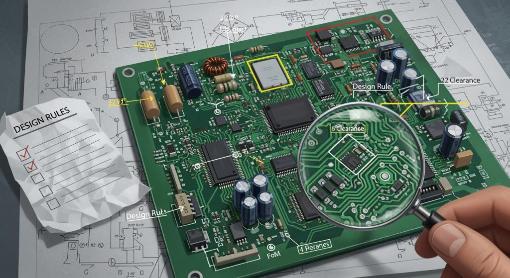
Improving Signal Integrity in RF PCB Design
Reducing Signal Loss with Design Tools
Signal loss can weaken how RF circuits work. To avoid this, use smart design methods and tools. Here are some simple strategies:
Use fewer vias when routing RF traces to keep signals strong.
Add a separate via for each RF component pin to protect signals.
Place multiple vias together to lower unwanted inductance and spread current evenly.
Put ground vias on RF traces to make good return paths.
Use via stitching to shorten ground paths and improve signal flow.
Work with your PCB maker to check via sizes and use back drilling to remove extra via parts.
3D electromagnetic (EM) simulation tools can also help. They show how electromagnetic fields behave and predict problems like interference before building the PCB.
Real-Life Ways to Improve Signal Integrity
These ideas can make RF PCB signals better. For example, keeping a solid ground plane near the signal reduces loop lengths. This lowers impedance and resistance. Adding a ground via close to each pad improves grounding even more.
Another way is controlling impedance. Pick the right dielectric thickness and copper weight to match target impedance. Simulation tools can check these settings for the best results.
Managing heat is also important. Good thermal control stops high-frequency designs from losing performance.
Tips for Using Tools Effectively
To get the most from RF PCB tools, try these tips:
Use 3D EM simulation to study signals and find problems early.
Check power integrity to keep voltage steady across the PCB.
Design antennas carefully to boost RF performance.
Write clear impedance rules in your notes and set tolerances for accuracy.
Talk often with your PCB maker to handle design changes and ensure everything works.
By following these steps, you can build RF PCBs that work well and keep signals strong.
Best Practices for RF PCB Layout Optimization

Placing Components in RF Circuits
Placing parts correctly is key in RF PCB design. Keep important parts like antennas and amplifiers close together. Shorter paths mean less signal loss and better performance. Keep sensitive parts away from noisy digital circuits to avoid problems.
Using simulations can improve your placement plan. Advanced methods, like special optimization tools, need fewer simulations but still work well. These tools help find layout issues and improve part placement for better results.
Heat control is also important when placing parts. Use copper areas to spread heat evenly and stop overheating. Separating analog and digital grounds reduces interference and keeps performance steady.
Routing Traces the Right Way
Routing traces is very important in RF PCB design. Controlled impedance routing keeps signals strong by making impedance steady. Route fast signals over solid ground planes to avoid changes in impedance. Don’t use sharp 90-degree turns; use smoother 135-degree bends instead.
Vias affect signal quality too. Use fewer vias to keep signals strong. Place ground vias near RF traces for good return paths. Via stitching helps signals flow better by shortening ground paths. Work with your PCB maker to adjust via sizes and use back drilling for better results.
Simulation tools can show how electromagnetic fields behave. They help find routing problems before making the PCB. Test different routing ideas to pick the best one for your design.
Ground Planes and Power Setup
Good ground planes are important for RF PCB design. Solid ground planes keep impedance steady and give stable return paths. Close power-ground planes lower impedance, letting more energy flow. Place decoupling capacitors near loads to make energy transfer faster.
Power setup affects how well the PCB works. Small capacitors improve energy use, and careful placement reduces interference. Use thermal reliefs to handle heat and protect parts from damage.
Ground planes also help signal strength. Adding ground vias near pads improves grounding and shortens loops. This lowers impedance and makes signals flow better. Following these tips helps you design better RF PCBs with reliable performance.
Testing and Improving Your RF PCB Design
Testing and improving are key steps in making your RF PCB work well. These steps help ensure your circuit works as planned and meets all needs. Testing early and often helps find problems and fix them before finishing the design.
Use Simulation Tools First
Simulation tools let you test your design virtually. They show how signals move through your PCB. Use them to spot problems like signal interference or impedance mismatches. Tools like 3D electromagnetic simulators can show electromagnetic fields and problem spots. Running tests with different settings gives a better idea of how your design performs.
Build and Test a Prototype
After simulations look good, make a physical prototype. Testing the prototype shows how your design works in real life. Use tools like a vector network analyzer (VNA) to check signal strength and losses. Watch how the ground plane affects signals and impedance. Testing in special rooms, like anechoic chambers, removes outside interference for better results.
Study Test Results
Look closely at test results to find areas to improve. Check for signal loss or interference patterns. If signals weaken near certain traces, try rerouting them or adding ground vias. Small layout changes can greatly improve performance.
Keep Testing and Improving
Improving your design takes many tries. After making changes, test again to see if problems are fixed. Repeat this process until your PCB works perfectly. Focus on fixing signal strength, impedance matching, and ground plane issues. Each test makes your design better and more reliable.
Work with Your Manufacturer
Your PCB maker can help during testing and improving. Share your test results and ask for advice. Manufacturers know a lot about designs like yours and can suggest helpful fixes. For example, they might recommend materials or methods to improve your ground plane or reduce signal loss.
Tip: Write down all tests and changes. Keeping records helps track progress and avoids repeating mistakes later.
By testing carefully and improving step by step, you can make an RF PCB that works well for any use. This process not only makes your design better but also helps you grow as a designer.
Learning RF PCB design and layout is key to making strong devices. Keeping signals clear and layouts smart helps meet standards and work well. Starting with easy tools like KiCad builds skills and boosts confidence.
“Keep learning because the PCB world keeps changing.”
Staying updated is important in the fast-changing PCB field.
Look into new tech like IoT and medical gadgets for new chances.
Join online talks and events to learn from experts and follow rules.
Meet people at conferences to share ideas and learn from others.
These habits will help you improve in RF PCB design and become a better designer.
FAQ
What is RF PCB design, and why does it matter?
RF PCB design makes boards for handling radio signals. It helps devices like phones and IoT gadgets work well. Good design reduces signal problems and makes devices reliable.
How can you stop signal interference in RF PCB layouts?
Keep traces short and use solid ground planes. Separate analog and digital parts to avoid issues. Simulation tools can find and fix problems before making the board.
What materials are best for RF PCBs?
Materials like Rogers or Teflon work well for high frequencies. FR-4 is cheaper and good for lower frequencies. Pick based on your project’s needs and budget.
How do you match impedance in RF circuits?
Use controlled impedance routing and calculate trace widths. Check the material’s dielectric constant. Simulation tools can confirm and adjust impedance values.
What tools are easy for beginners in RF PCB design?
KiCad is free and simple to use. It has lots of online help. Other tools like Eagle and Altium Designer have more features but need more experience.