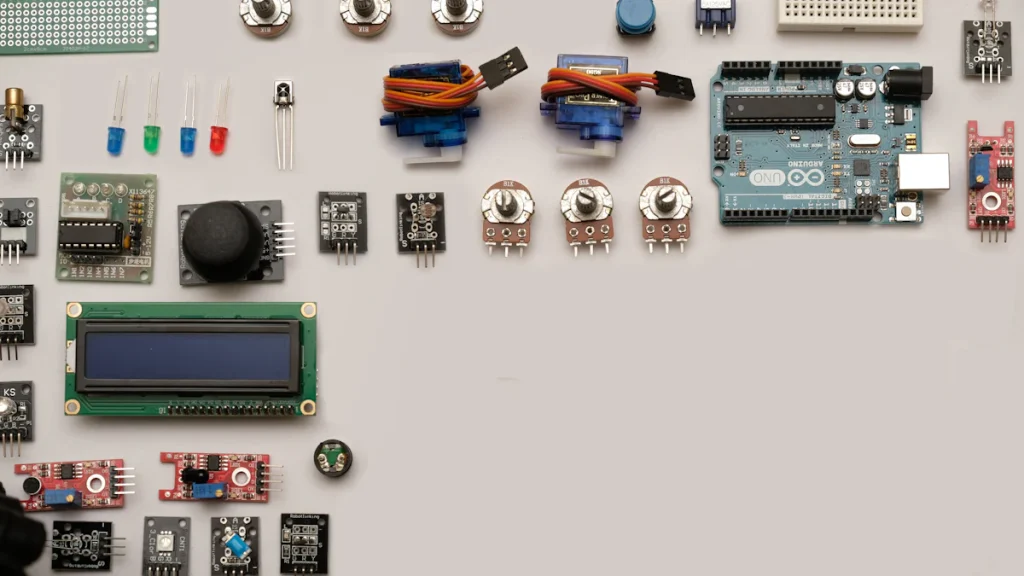
Designing RF PCBs is important for modern technology like phones and car radar. These boards work with signals over 1GHz to keep them clear and strong. Unlike regular PCBs, RF boards need special materials to avoid signal loss at high speeds. You must solve problems like matching signal paths, stopping signal bounce, and blocking unwanted noise. Careful planning and following good design rules are key for success. Learning RF PCB design helps create advanced and exciting technologies.
Key Takeaways
RF PCB design works with high-frequency signals over 1 GHz. It’s important to reduce noise and keep signals clear.
Picking the right materials is very important. Use materials with stable properties and low energy loss to avoid signal problems.
Controlling impedance is key for RF PCBs. Make sure trace widths and spaces keep a steady 50-ohm impedance to stop signal issues.
Try simulation tools to check your design before making it. This finds problems early and ensures the PCB works well in real life.
Follow rules and guidelines to make it reliable. Place parts carefully and use shielding to lower electromagnetic interference.
Understanding RF PCB Design Basics

What is RF PCB Design
RF PCB design is about making circuit boards for high-frequency signals, usually above 1 GHz. These boards are used in things like wireless devices, radar, and IoT gadgets. Unlike regular boards, RF designs need exact control of signal paths and impedance to keep signals clear.
Important parts of RF PCB design include:
Reducing noise to stop ringing and signal echoes.
Keeping a steady 50-ohm impedance across the board.
Lowering return loss for better signal flow.
You also need to plan the return signal path carefully. This avoids problems with mismatched impedance. As boards get more crowded, crosstalk becomes a bigger issue. To fix this, you must space traces properly and plan layouts well.
Tip: Focus on matching impedance and cutting noise for better RF results.
Key Differences Between RF and Standard PCB Design
RF PCBs are different from regular PCBs in key ways. The dielectric constant (Dk) of the material is very important in RF design. It affects how signals behave. But Dk values can change between manufacturers because of different testing methods. This makes picking materials harder.
RF designs also react more to material properties at higher frequencies. For example, laminate materials affect both the traces and the board’s electrical performance. This is even more critical in precise systems like military applications.
Note: Check Dk values from manufacturers and understand their testing methods before choosing materials.
High-Frequency Signal Behavior in RF PCB Boards
High-frequency signals in RF PCBs act differently and need special care. Small parts like resistors and capacitors can behave unpredictably at high frequencies. For instance, resistors may not match their labeled values at around 10 GHz.
To handle this, use detailed data like impedance graphs or S-parameter charts. These tools show how parts work at certain frequencies. This helps you design more accurately and avoid surprises.
Tip: Use data to check part performance and prevent signal issues.
Key Considerations for High-Frequency Applications
Material Selection for RF PCB Boards
Picking the right materials is very important for RF PCB boards. Materials need steady electrical properties, especially at high frequencies. The dielectric constant (Dk) helps signals move through the board. A stable Dk makes signals act predictably, which is key for high-frequency use. The dissipation factor (Df) shows energy loss. Materials with low Df reduce signal weakening.
Heat is another thing to think about. High-frequency signals create heat that can change material properties. This hurts performance. Materials like PTFE laminates handle heat and keep electrical properties steady. These are often used in RF devices like base stations.
Tip: Check material specs like Dk, Df, and heat stability from manufacturers.
Key things to check include:
Dielectric constant (Dk)
Dissipation factor (Df)
Signal loss
Impedance control
Heat management
Impedance Control and Its Importance
Impedance control is very important in RF design. It keeps signals moving without bouncing or losing strength. If impedance doesn’t match, signals bounce back and cause problems. RF boards need steady impedance, usually 50 ohms, for best results.
Impedance tests show if the board matches expected values. Good impedance control stops signal bouncing and improves electromagnetic compatibility. For example, it reduces electromagnetic interference (EMI), which helps RF circuits work better.
To control impedance, design trace widths, spacing, and layers carefully. Simulation tools can predict impedance and help improve the design before making the board.
Note: Impedance control is a must for RF boards. It affects signal quality and circuit performance.
Signal Integrity and Electromagnetic Interference (EMI)
Signal integrity and EMI are connected in RF design. High-frequency signals can easily get interference, which messes up signals. When traces are close, crosstalk and noise happen more often. To fix this, keep traces apart and use shields like ground pours and via stitching.
For example, ground pours and via stitching can cut coupling by 20 dB. This improves signal integrity by 100 times. Shielding cans, which cover most of the PCB, also block interference. But small designs may not have space for these.
Heat noise and RF path loss also hurt signal integrity. Fix these by improving layouts and using parts made for high frequencies. Simulation tools help find problems and check your design.
Tip: Use shielding and good layouts to protect signals and lower EMI.
Layer Stack-Up Design for RF PCBs
The layer stack-up in an RF PCB is very important. It shows how copper and dielectric layers are arranged. This affects signal quality, impedance control, and electromagnetic interference (EMI).
Why Layer Stack-Up is Important
The stack-up decides how signals move through the board. A bad stack-up can cause signal loss, crosstalk, and EMI. Planning the layers well helps avoid these problems. It also keeps RF circuits working reliably.
Tip: Think about frequency and material properties when planning the stack-up.
Main Parts of an RF PCB Stack-Up
When designing the stack-up, focus on these parts:
Signal Layers: These carry high-frequency signals. Keep them close to the ground plane to lower noise and improve signal quality.
Ground Planes: These give signals a reference and control impedance. A full ground plane helps reduce EMI.
Dielectric Layers: These separate copper layers and affect the board’s Dk. Pick materials with steady Dk for better signal behavior.
Power Planes: These spread power across the board. Putting them near ground planes adds decoupling capacitance, which cuts noise.
Tips for Good Layer Stack-Up Design
Use these tips to make a strong stack-up for your RF PCB:
Use Fewer Layers: Only use the layers you need to save money. But make sure to separate signal and power planes properly.
Keep It Symmetrical: A balanced stack-up stops the board from bending during manufacturing.
Control Impedance: Design layers to keep impedance steady for high-frequency signals. Use tools to check impedance values.
Add Shielding: Place ground planes to protect signal layers from interference.
Example of a Simple RF PCB Stack-Up
Here’s an example of a 4-layer RF PCB stack-up:
Layer Number | Function | Description |
|---|---|---|
1 | Signal Layer | Carries high-frequency signals |
2 | Ground Plane | Controls impedance and reduces EMI |
3 | Power Plane | Spreads power across the board |
4 | Signal Layer | Extra space for signal routing |
This setup keeps signals clear and lowers EMI.
Note: For complex designs, add more layers to separate signals and power planes.
Tools for Stack-Up Planning
Use software like Altium Designer or KiCad to design your stack-up. These tools let you test your design and fix problems before making the board.
By planning the layer stack-up carefully, you can make RF PCBs work better for high-frequency uses. This step is key to avoiding signal problems and ensuring good performance.
Step-by-Step Process to Design RF PCB
Define Design Requirements and Specifications
Before starting, set clear goals for your RF PCB. These goals act like a guide to help your design meet performance needs. Focus on important factors to make good decisions.
Key Performance Indicator | Description |
|---|---|
Impedance Control | Keeps signals clear and reduces losses in fast circuits. |
Signal Integrity | Ensures reliable signals and fewer errors in data transfer. |
Material Selection | Affects how well the board works, including heat and signal loss. |
To meet these goals:
Test and simulate your designs often to check performance.
Plan the layout carefully to keep signals strong.
Use methods to lower electromagnetic interference (EMI).
Tip: Make a checklist of your goals before you start. This helps you stay focused and avoid mistakes.
Select Materials and Components for RF PCB Boards
Picking the right materials and parts is very important. The materials you choose affect how the board works, especially at high speeds. Look for materials with steady dielectric constants (Dk) and low dissipation factors (Df). These help signals stay clear and reduce energy loss.
For example, PTFE laminates are great for RF boards because they handle heat well and lose less signal. When choosing parts, check how they work at high frequencies. A resistor might not work as expected at 10 GHz. Use data sheets with graphs to confirm how parts perform.
Note: Talk to manufacturers to make sure materials and parts fit your needs.
Things to think about when picking materials and parts:
How steady the Dk and Df values are.
If they can handle heat without problems.
If they match your design’s impedance needs.
Create the PCB Layout with RF Considerations
The layout is where your design becomes real. Following good layout rules is key to making your RF PCB work well. Keep high-frequency traces short and direct. This lowers signal loss and interference.
Use ground planes to give signals a steady base and control impedance. Placing signal layers near ground planes improves signal quality and cuts interference. Add via stitching and ground pours to protect sensitive areas even more.
Tip: Advanced layout methods can improve performance by 10 to 30 times. Try new techniques to make your design better.
Other layout tips include:
Keep trace widths the same to control impedance.
Separate high-frequency traces from power and ground to avoid crosstalk.
Use simulation tools to check your layout before making the board.
By planning your layout well, you can avoid problems like signal issues and EMI. This ensures your RF PCB works well in high-frequency situations.
Simulate and Validate the RF PCB Design
Testing your RF PCB design with simulations is very important. It helps find and fix problems before making the board. This saves both time and money. Simulations show how high-frequency signals behave and check if the design works well.
Why Simulation is Important
High-frequency signals are sensitive to layout and materials. Without testing, you might face signal loss or interference. Simulation tools let you spot these problems early. You can adjust your design to avoid issues like mismatched impedance.
Main Simulation Methods
Try these methods to test your RF PCB design:
EM Simulation: Check signal quality and noise using special tools. These tools show how signals interact with the board’s layout.
S-Parameter Analysis: Test how signals behave at different frequencies. This ensures your design works for the needed frequency range.
Time Domain Reflectometry (TDR): Check trace impedance and find any breaks. TDR helps keep impedance steady across the board.
Network Analysis: Use tools to measure how well RF circuits work. These tools give detailed information about signal behavior.
Tip: Use more than one simulation method for better results.
Features to Look for in Simulation Tools
Pick tools with these features for better testing:
Options to match impedance in signal paths.
Tools to check specific parts of the design.
Combined routing and layout tools in one program.
Simulation tools also help find noise and power issues. For example, they can check stackups and power stability. This helps improve your design and fix weak spots.
Note: Always test your design under real-world conditions for accuracy.
Manufacture and Test the RF PCB Board
Once your design is ready, it’s time to make and test the board. This step ensures the RF PCB works well and meets quality standards.
Making the RF PCB
Work with your manufacturer to match your design needs. Share clear details like material types and impedance goals. This reduces mistakes during production.
To check quality, make a few sample boards first. Produce 5–25 boards to test how consistent they are. This helps find any problems in the manufacturing process.
Testing the RF PCB
Testing makes sure your RF PCB works as planned. Follow these steps to test it:
Proof of Design Tests: Check if the board works correctly. Test signal quality, impedance, and noise levels.
Design for Manufacturing (DFM): Make sure the design is easy to produce. Fix anything that could cause trouble during manufacturing.
Design for Testability (DFT): Add features like test points to make testing easier.
Test all sample boards for function, electrical performance, and durability. Use the results to fix any design problems before full production.
Following Standards
Follow industry rules when testing RF PCBs. For example, use MIL-STD-810 for vibration tests. Make sure your board meets safety and noise standards.
Tip: Test your board in real-world conditions to find hidden problems.
By testing carefully, you can ensure your RF PCB works well in high-frequency applications. This step is key to delivering a reliable product.
Common Challenges in RF PCB Design
Managing Crosstalk and EMI
Crosstalk and EMI are big problems in RF PCB design. Crosstalk happens when signals from nearby traces mix together. This causes noise and messes up the signal. EMI is caused by unwanted electromagnetic waves that hurt circuit performance. Both issues can weaken signals and make your RF system less reliable.
To fix crosstalk, keep enough space between high-frequency traces. Use ground planes and via stitching to protect sensitive areas. For EMI, add shields like metal covers or ground pours to block interference. A good ground plane lowers coupling and boosts performance.
Bad EMI designs can cause major issues. Reports show shielding and resonance analysis help reduce interference.
By solving these problems early, your RF PCB can work reliably and consistently.
Ensuring Accurate Impedance Matching
Impedance matching is very important for RF PCBs. It helps send the most power between the source, line, and load. If impedance doesn’t match, signals bounce back, wasting power and lowering efficiency. Matching impedance keeps signals clear and reduces distortion.
Use tools to design traces with steady impedance. Tapered trace transitions can match impedance across different PCB sections. Make sure the transmission line’s impedance equals the source and load impedance.
Impedance matching is key for RF systems. Mismatched impedance reflects signal power, hurting efficiency.
By focusing on impedance matching, your RF PCB will work better for high-frequency tasks.
Addressing Thermal Issues in High-Frequency Applications
High-frequency circuits create a lot of heat, which can hurt performance. Too much heat weakens signals and damages components. Good heat management keeps your PCB reliable.
Use thermal vias to move heat away from hot parts. Thermal interface materials help spread heat, especially in RF systems with powerful components. Simulations predict heat levels and find hot spots. Place parts and vias carefully to improve heat control.
Strategy | Description |
|---|---|
Thermal Interface Materials | Help spread heat in high-frequency systems. |
Thermal Vias | Move heat away from hot components. |
Thermal Simulations | Predict heat levels and find problem areas. |
RF amplifiers create heat that affects performance. Simulations and tests help keep temperatures safe.
By using these methods, you can handle heat problems and make your RF PCB last longer.
Avoiding Signal Loss and Distortion
Signal loss and distortion can hurt how well RF PCBs work. High-frequency signals are more likely to have these problems. You can reduce them by using smart design methods.
Keep signal paths short and straight. Long paths weaken signals and cause distortion. Controlled impedance helps signals move smoothly without bouncing or breaking.
Back drilling is useful for fixing interference. It removes extra parts of vias, stopping nearby lines from affecting each other. This lowers crosstalk and keeps signals separate. Back drilling also improves signal flow by fixing impedance breaks. It helps signals stay clear in RF and microwave devices.
Good grounding is very important. A full ground plane gives signals a steady base and cuts electromagnetic noise. Via stitching connects PCB layers and stops noise from spreading. This keeps signals clean and strong.
Shielding parts can block outside interference. Metal covers or ground pours protect circuits from noise. Keeping high-frequency paths apart also stops signals from mixing and getting distorted.
Simulation tools are helpful for testing designs. They show problems before making the board. This ensures the PCB works well in real-world conditions.
Using these tips can stop signal loss and distortion. Your RF PCB will work better and stay reliable.
Tools and Resources for RF PCB Design
Recommended Software for RF PCB Design
Picking the right software makes RF PCB design easier. It also helps you create accurate designs. Many programs have special features for high-frequency projects. Below is a list of popular tools:
Tool Name | Description |
|---|---|
Altium | Combines all needed tools in one place, saving time. |
Microwave Office | Easy to use and great for high-frequency designs. |
PADS | Best for simple designs with easy layout and schematic tools. |
Cadence | Includes tools for designing chips and advanced circuits. |
HFSS | Top choice for simulating 3-D electromagnetic fields accurately. |
Electronics Workbench | Popular for circuit simulation, used by over 180,000 people. |
Advanced Design System | Leading tool for RF and microwave designs with modern features. |
L-Edit | Helps with efficient IC physical design. |
S-Edit | Makes creating complex schematics easier and faster. |
Ansoft Designer | Combines circuit, system, and electromagnetic simulations for high-frequency projects. |
These tools suit different needs, from basic layouts to advanced simulations. Choose based on your project’s difficulty and frequency needs.
Tip: Beginners can try Altium or Microwave Office. For detailed simulations, use HFSS.
Online Tutorials and Learning Resources
To learn RF PCB design, use trusted resources. Online courses and videos explain important topics step by step. Websites like YouTube, Coursera, and Udemy teach things like impedance control and EMI reduction. Many software companies also offer guides and webinars for their tools.
For practical advice, visit forums like PCBWay or Stack Exchange. These platforms let you ask questions and learn from experts. Blogs and whitepapers from companies like Keysight and Rogers Corporation also provide deep insights into RF materials and testing.
Tip: Save helpful resources and revisit them as you improve your RF PCB skills.
Industry Standards and Guidelines for RF PCB Boards
Following industry rules ensures your RF PCB works well and lasts long. These guidelines help you design circuits that perform reliably in high-frequency settings.
Key Design Tips:
Component Placement: Place RF parts to reduce unwanted effects and shorten paths.
Material Selection: Use low-loss materials like Rogers laminates for better signals.
Transmission Lines: Use microstrips or striplines to keep impedance steady.
RF Testing: Test thoroughly to confirm your design meets requirements.
EMI/EMC: Add shields and filters to block interference.
Important Standards:
IPC-6012: Explains tests for stability and moisture resistance.
IPC-2221: Gives general design rules for reliable PCBs.
IPC-A-600: Lists quality checks for PCB manufacturing.
Using these standards helps you build RF PCBs that meet industry needs. They also ensure your designs work well in tough conditions.
Note: Check for updates to stay current with the latest rules.
Making RF PCBs for high-frequency use needs careful planning. You should pick the right materials, control impedance, and keep signals clear. Using simulation tools helps check if your design works well. For instance, comparing numbers can show how accurate your design is. See the table below for examples:
Validation Step | What It Means |
|---|---|
Simulating PCB Parts | Tested PCB parts with specific trace sizes and material models. |
Comparing S-parameters | Checked measured and tested S-parameters for accuracy. |
Time-domain Testing | Looked at time-based results to find any problems. |
Results Overview | Found less than 2% difference in 30 Gbps tests, with issues above 30 GHz due to part placement. |
Use these tips to improve your designs. Keep learning new methods to stay ahead in RF PCB design. This helps your boards work better and stay useful for high-frequency tasks.
FAQ
1. What matters most in RF PCB design?
Signal integrity is very important. Keep signal paths clear and impedance matched. Stop interference by using good materials and smart layouts. Shielding also helps keep signals strong.
2. How do I pick the best material for RF PCBs?
Choose materials with steady dielectric constant (Dk) and low dissipation factor (Df). These features lower signal loss and boost performance. PTFE laminates are great for high-frequency use because they resist heat and work reliably.
3. Why is impedance control so important?
Impedance control stops signals from bouncing back or getting weak. It helps signals move smoothly across the board. Use tools to plan trace sizes and spacing. Test impedance during design to avoid problems.
4. How can I block electromagnetic interference (EMI)?
Use ground planes, shielding cans, and via stitching to stop EMI. Keep high-frequency traces short and spaced apart. Filters and decoupling capacitors also help reduce interference.
5. What software works best for RF PCB design?
Altium Designer and Microwave Office are good for beginners. HFSS is better for advanced users needing detailed simulations. Pick software based on your project’s needs and frequency level.