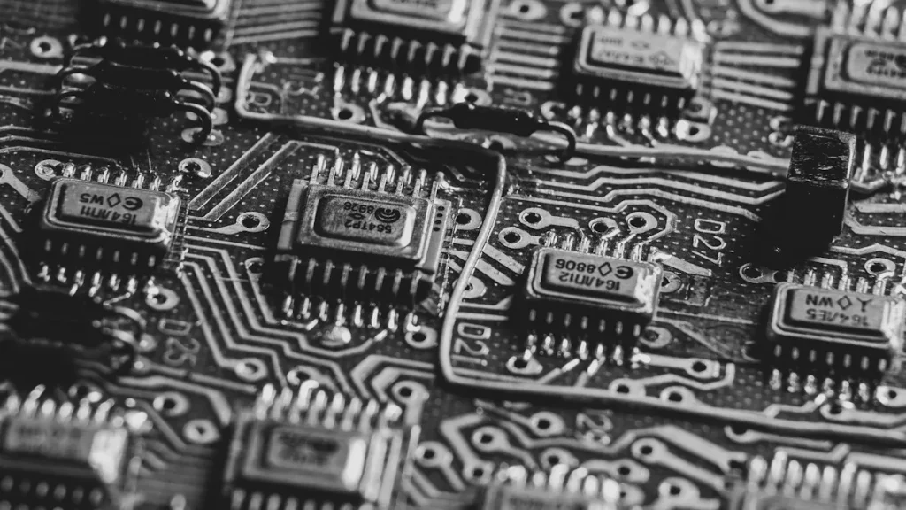
Mistakes in RF PCB design can cause big problems. If high-frequency signals are not handled well, they can create heat. This heat can harm parts of the board. Using tools like heat sinks or thermal vias helps stop this. Also, bad trace routing or no shielding can cause interference. This can mess up how the board works.
Making RF PCBs is tricky. You must keep signals strong and reduce interference. Even small mistakes, like bad grounding or poor trace paths, can damage the board over time. To do it right, follow smart tips and good design steps.
Key Takeaways
Matching impedance is very important. Make sure transmission lines and connected parts have the same impedance to avoid signal problems and losing power.
Grounding helps your design work better. Use a strong ground plane to lower noise and interference. Don’t split the ground plane so current flows smoothly.
Keeping signals clear matters in high-frequency designs. Use simulation tools to find problems like crosstalk or EMI. Make sure trace widths and spaces are even.
Placing parts smartly makes designs better. Put related parts close together to make signal paths shorter and reduce interference. Keep sensitive parts away from noisy ones.
Learn about new RF design ideas. Knowing new materials and methods can improve your designs and prepare them for future needs.
Common Mistakes in RF PCB Design
Poor Impedance Matching and Its Impact
Impedance matching is very important in RF PCB design. If the impedance of a transmission line doesn’t match connected parts, problems happen. Signals can bounce back, causing ringing and distortion. These issues get worse at higher frequencies. Even small mismatches can mess up signal flow. For example, bouncing signals from connectors can cause big inductive effects. This makes accurate measurements harder. Keeping probe wires short helps reduce these problems.
Bad impedance matching also slows down signal rise time and settling. As signals move through cables, their strength can change. This happens if the device’s impedance isn’t what it should be, like 50 ohms. Such mismatches can cause errors in accuracy, which are crucial for RF tasks. To prevent this, always match impedance correctly during design.
Inadequate Grounding in RF PCB Boards
Good grounding is key for RF PCB performance. Without it, noise and interference can ruin signals. A bad grounding setup can create loops that add unwanted noise. This noise disrupts RF signals and lowers the board’s performance.
To fix this, use a solid ground plane. This lowers the impedance of return paths and stops signal distortion. Don’t split the ground plane too much, as it can isolate sections and block current flow. Add vias carefully to connect PCB layers, giving return currents a clear path. Proper grounding improves signal quality and makes your design more reliable.
Overlooking Signal Integrity in High-Frequency Designs
Signal integrity matters a lot in high-frequency designs. Small mistakes can cause big problems. Bad trace routing can lead to signal bouncing, crosstalk, and electromagnetic interference (EMI). These issues weaken signals and hurt circuit performance.
One mistake is uneven trace widths and spacing. Changing trace shapes can affect impedance and distort signals. Also, traces placed too close can cause crosstalk, where signals mix and interfere. This is worse in crowded PCBs.
To solve these problems, use simulation tools to check signal integrity. These tools find issues and help improve layouts for high-frequency use. By focusing on signal integrity, your RF PCB will work well, even in tough conditions.
Inefficient Component Placement in RF Layouts
Bad placement of parts can hurt RF circuit performance. If parts are too close or far, signal paths get longer. Longer paths can cause extra capacitance and inductance, which distort signals. Misplaced parts can also make signals mix and interfere.
To fix this, place parts in a smart way. Group parts by what they do. For example, keep amplifiers, filters, and oscillators near each other. This shortens important signal paths. Put sensitive parts, like low-noise amplifiers, away from noisy ones, like power regulators. This helps stop interference.
Align parts with the signal flow for better layouts. This makes tracing signal paths easier. Use simulation tools to test your design before finishing it. These tools find problems like signal delays or interference early.
Tip: Check component datasheets for placement advice. They often suggest the best spacing and layout.
Planning your layout well ensures your RF design works smoothly and reliably.
Neglecting EMI and Crosstalk Mitigation
EMI and crosstalk are big problems in RF circuits. EMI happens when outside signals mess up your circuit. Crosstalk occurs when signals from one path interfere with another. Both can weaken signals and hurt circuit performance.
To reduce EMI, use shields over sensitive parts. Metal shields block outside signals. Ground the shield properly to make it work well. Keep high-frequency paths away from noisy parts like switching regulators.
For less crosstalk, leave enough space between signal paths. Avoid running paths side by side for long distances. Instead, cross them at right angles when you can. Add ground paths between signal traces to stop interference.
Note: High-frequency signals are more likely to have EMI and crosstalk. Pay extra attention to these areas.
Fixing EMI and crosstalk early makes your RF circuit more reliable and keeps signals strong.
Practical Solutions for Designing RF PCB Boards
Ways to Ensure Proper Impedance Matching
Impedance matching helps signals move smoothly in RF circuits. If impedance doesn’t match, signals bounce back. This causes distortion and power loss. To fix this, focus on the design of transmission lines and connected parts. Use tools like Smith charts to see and adjust impedance. Matching networks, like LC circuits or quarter-wave transformers, can align impedance values well.
Keep trace widths the same to avoid problems. Uneven widths can block signals and cause reflections. Use controlled impedance traces for high-frequency signals. These traces match the impedance of connected parts, reducing signal issues. Avoid sharp trace bends, as they change impedance and hurt signal quality.
Tip: Test impedance matching early with simulation tools. This finds problems fast and avoids expensive fixes later.
Grounding Tips for RF PCB Design
Good grounding is very important in RF PCB design. A solid ground reduces noise and keeps signals strong. One way is to use a continuous ground plane. This gives signals a clear return path and lowers electromagnetic interference (EMI). It also makes the loop area between signal and return paths smaller, improving performance.
Here are some grounding tips:
Star Grounding: Connect sensitive parts to one ground point. This lowers noise and keeps signals clean.
Ground Vias: Spread return currents across PCB layers evenly. This lowers impedance and helps high-speed signals.
Short Ground Paths: Shorter paths lower resistance and inductance, keeping signals clear.
A telecom company used these tips by adding a solid ground plane and star grounding. This cut noise and improved system performance a lot.
Note: Don’t split the ground plane too much. Splits can block current flow and distort signals.
Using Simulation Tools for Signal Integrity
Simulation tools are key for keeping signals strong in RF PCB design. Tools like HFSS and ADS let you make virtual circuit models. These models show how circuits work and find problems before building them.
With these tools, you can check electromagnetic fields and signal paths. They help find issues like impedance mismatches, crosstalk, and EMI. For example, you can test different trace sizes and part placements to improve signal flow. Testing again and again ensures your design works well without wasting money.
Simulation tools also show how signals act at high frequencies. They let you see how signals interact with PCB materials and layouts. By using these tools, you can improve your design and make it work well in real life.
Tip: Update your simulation tools often. New features make designs better and more accurate.
Optimizing Component Placement for RF Performance
Placing parts correctly is key for good RF PCB design. When parts are placed smartly, signal paths stay short and direct. This lowers unwanted capacitance and inductance, improving signal quality. Group parts by their job. For example, keep amplifiers, filters, and oscillators close together. This helps signals flow better. Keep sensitive parts, like low-noise amplifiers, away from noisy ones, such as power regulators.
Good placement also helps manage heat. Place heat-making parts, like power regulators, near heat sinks or thermal vias. This stops overheating and makes your PCB last longer. Align parts with the signal flow to make routing easier and reduce distortion. Use simulation tools to test layouts and find problems before finishing the design.
Here’s how better placement improves performance:
Performance Metric | Benefit Description |
|---|---|
Signal Integrity | Smart placement avoids signal issues, saving time later. |
Electromagnetic Interference (EMI) | Careful design lowers EMI, preventing future problems. |
Thermal Management | Good heat control stops overheating and extends part life. |
Ground Planes | Solid ground planes keep signals stable and strong. |
By focusing on these points, you can design a PCB that works well and lasts longer.
Designing for EMI Reduction and Noise Immunity
Cutting EMI and blocking noise are vital for RF PCB designs. EMI can mess up signals, and noise can harm sensitive parts. To fix this, use shields. Metal shields over sensitive parts block outside signals. Ground the shields properly to make them work better.
Spacing between traces is also important. Traces too close can cause crosstalk, where signals mix and interfere. Leave more space between traces or cross them at right angles. Adding ground paths between traces also helps stop interference.
Studies show advanced EMI fixes work well. For example:
Study | Technique | Findings |
|---|---|---|
Y Liu et al. | Deep Learning Model | Predicted and removed EMI, matching RF shielding results. |
Y Zhao et al. | Active Sensing and Deep Learning | Used sensing coils and AI to cancel EMI in MRI scanners without shields. |
These studies prove new methods can improve RF performance without just using shields. Combine these ideas with smart PCB design to lower EMI and block noise.
Tip: Test for EMI and noise early with simulation tools. Fixing problems early saves time and money later.
Best Practices for RF PCB Design
Working with RF Experts Early in the Process
Getting help from RF experts early can save time and money. These experts know a lot about signals, interference, and high-frequency problems. Their advice helps your design work well and avoids common errors.
You can ask RF experts to help pick materials, plan trace paths, and design grounding. They can also explain simulation results and suggest fixes. Working together at the start makes the design process smoother and reduces changes later.
Tip: Meet with RF experts often to find and fix problems early.
Following Industry Rules and Guidelines
Using standard RF PCB design rules makes your board work better. These rules show how to reduce interference and improve signal quality. Some important tips include:
Plan layouts to avoid interference and signal mixing.
Place parts like amplifiers and filters in smart spots.
Use good ground planes to block interference.
Match trace impedance to stop signal bouncing.
Use paired routing to reduce signal mixing.
By following these rules, your design will meet both performance and safety standards.
Note: Following rules also makes it easier to get your PCB certified.
Picking the Right Materials for RF PCB Boards
Choosing good materials is key for strong RF PCB performance. The materials you use affect signals, heat control, and reliability. For example, the dielectric constant (Dk) of a material affects signal speed. Low and steady Dk values help signals move better.
Here are some material tips and their effects:
Material Feature | How It Helps | Extra Info |
|---|---|---|
Dielectric Thickness | Controls impedance and power loss | Important for handling power |
Conductor Width | Affects power flow | Must fit the circuit needs |
Thermal Properties | Helps manage heat | Picks materials that cool well |
Smooth copper reduces signal loss, and special plating works best for high frequencies. Knowing about things like skin effect and loss tangent helps you pick materials that lower noise and signal loss.
Tip: Check material datasheets to make sure they fit your design needs.
Conducting Comprehensive Testing and Validation
Testing makes sure your RF PCB works well. It helps find and fix problems before production. This improves performance and saves money by avoiding failures.
Here are key testing steps:
Prototype Testing: Build and test models to check how they work.
Signal Integrity Analysis: Use tools to spot signal issues like distortion.
Environmental Testing: Test for heat, cold, or shaking to ensure strength.
These methods lower failure rates:
In aerospace, testing made prototypes 30% more reliable.
In electronics, validation cut failures by half.
In cars, better layouts saved 20% on prototype costs.
Testing ensures your PCB works well in different conditions.
Tip: Write down your testing steps. This helps track fixes and find repeated problems.
Staying Updated on RF PCB Design Trends and Innovations
Learning about new RF PCB trends keeps you ahead. New ideas change how circuits are made and improved. For example, better materials and methods boost PCB performance.
Here’s how trends affect designs:
Trend | How It Helps |
|---|---|
Rise of 5G | Needs PCBs that handle faster data and more bandwidth. |
Growth of IoT | Requires smaller, cheaper, and better PCBs for many uses. |
Changes in Cars | Demands strong PCBs for radar, lidar, and sensors in self-driving cars. |
Better Materials | Improves signals and allows more parts with advanced laminates and HDI tech. |
Focus on Signal Integrity | Needs better designs and tests to stop EMI and improve reliability. |
Knowing these trends helps you design for today’s needs. For example, 5G needs PCBs for faster data. New materials improve signals and reduce interference.
Note: Read industry news or join webinars to learn about new ideas.
Avoiding errors in RF PCB design makes boards work better. Fixing problems like impedance mismatches and EMI early saves time. It also stops delays during production. Careful checks during design prevent big mistakes. These include wrong schematics or missing parts. Fixing these issues helps manufacturers accept your design without problems.
Using smart solutions and good practices makes designs reliable. Follow industry rules to ensure strong performance. Learn new methods and RF trends to stay ahead. This keeps your designs ready for future needs and working efficiently.
FAQ
What matters most in RF PCB design?
Impedance matching is very important. It keeps signals moving smoothly and stops reflections. Bad matching can mess up signals and waste power. Use tools like Smith charts and special traces to match impedance correctly.
Tip: Test impedance early to avoid expensive mistakes later.
How do you lower EMI in RF PCB designs?
Cover sensitive parts with metal shields and use good grounding. Keep high-frequency paths away from noisy parts. Add ground paths between traces to block interference.
Note: Leave space between traces or cross them at right angles to reduce crosstalk.
Why is grounding important for RF PCB boards?
Grounding gives signals a steady base and cuts noise. A solid ground plane makes signals clearer and reduces EMI. Without good grounding, your circuit might not work well.
Tip: Don’t split the ground plane to keep current flowing smoothly.
What tools help keep signals strong in RF PCB design?
Simulation tools like HFSS and ADS are very helpful. They let you test circuits, check electromagnetic fields, and find problems like mismatched impedance or crosstalk before making the board.
Emoji: 🛠️ Use these tools early to save time and improve your design.
How do you pick the best materials for RF PCBs?
Choose materials with low and steady dielectric constants (Dk) for better signal speed. Smooth copper lowers signal loss. Look for materials that handle heat well.
Material Feature | How It Helps |
|---|---|
Low Dk | Speeds up signals |
Smooth Copper | Cuts signal loss |
Thermal Stability | Manages heat better |
Tip: Read datasheets to find materials that fit your design.