To reverse engineer a pcb, first look at the board closely. Write down each part you see. Use tools like cameras and multimeters to find where the traces go. You must write down everything you do. You also need to know the laws at every step.
Tip: Always check legal rules before you start.
Legal Consideration
Description
Intellectual Property
Copyrights, patents, and trade secrets may protect the board design.
Ownership and Intent
You must own the board and use reverse engineering for repair, research, or learning.
Electronic reverse engineering lets you fix, upgrade, or learn about a circuit board. Many people use reverse engineering to get better at their jobs. It helps them make better products. If you follow each step in order, you will do well.
Key Takeaways
Always make sure you follow the law and own the board before you start reverse engineering. This helps you stay safe and fair.
Use the right tools like cameras, microscopes, and software. These help you look closely and record every part and line on the board.
Set up a clean and safe workspace. Use the right protection so you do not break anything and can work well.
Take clear pictures of both sides of the board. Write down good notes to help you follow the paths and make correct schematics.
Test and check all the connections with tools like multimeters and oscilloscopes. This helps you find and fix problems easily.
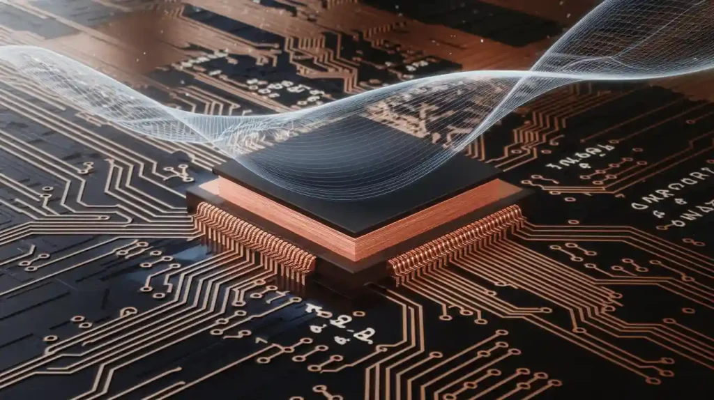
Electronic Reverse Engineering Overview
What Is Reverse Engineering?
Electronic reverse engineering helps you learn how a board works. You take the board apart and look at each part. You follow every trace and connection to see how it works. This lets you understand the design and layout of the board. You can use this skill to fix boards or make them better. It also helps you learn new ways to work with boards. With electronic reverse engineering, you can see how your devices work inside.
Why Reverse Engineer a Circuit Board?
There are many reasons to reverse engineer a pcb. Sometimes, you need to fix a board when parts are missing. You might want to check if a board is fake or real. You may want to see how another company’s board works. You can also find ways to make your own boards better. Here are some reasons people do pcb reverse engineering:
Swap out old parts so boards keep working.
Find fake products and stop hardware attacks.
Check designs and fix problems during building.
Make boards better and improve how they are made.
Look at other boards to get new ideas.
Note: Always follow the law and be fair when you reverse engineer a board. You must own the board and respect others’ rights. Laws like copyright, patent, and trade secret rules protect many boards. Some contracts may say you cannot reverse engineer. The table below shows some important legal and ethical rules:
Legal/Ethical Aspect | Key Points |
|---|---|
Copyright Law & DMCA | Only let you reverse engineer for things like research or making things work together. |
Trade Secret Law | You must be fair and honest. |
Contract Law | Some deals do not allow reverse engineering. |
Patent Law | Patents protect inventions. Do not break these rules. |
Ethics | Be honest and respect the people who made the board. |
Electronic reverse engineering helps you fix problems and learn new things. When you follow the rules, you help new ideas grow and respect others’ work.
Tools and Preparation

Essential Tools for Reverse Engineering
You need special tools to start reverse engineering a circuit board. Each tool helps you look at the board in a different way. Some tools help you see small parts. Others help you measure or record what you find. Professionals use these tools at every step. The table below shows the main types, examples, and how often you use them:
Tool Category | Tools Included | Usage Frequency and Purpose |
|---|---|---|
Hardware Tools | Desoldering stations, rework stations, signal analyzers, oscilloscopes, microscopes, imaging systems, X-ray machines | Used a lot for taking off parts, checking layers, and taking pictures. |
Software Tools | Image processing tools, PCB layout software, schematic capture tools, circuit simulation software | Used often for making notes, drawing the board, and checking your work. |
Advanced Technologies | 3D scanning, AI, automated reverse engineering tools | Used for hard boards. These tools help but do not replace the main tools. |
You will use these tools many times while working. You might need a camera to take clear pictures. A microscope helps you see tiny lines. PCB design software lets you draw what you find. Always pick the right tools for your board’s size and how hard it is.
Setting Up for Circuit Board Analysis
A clean and safe workspace helps you avoid mistakes. It also keeps you healthy. Follow these steps to get ready:
Wear gloves and coveralls to keep your skin safe from dust and chemicals.
Use safety glasses or goggles to protect your eyes when taking off parts.
Work in a place with fresh air. Use fans or open windows so you do not breathe in fumes.
Always turn off and unplug the board before you start. Take out any batteries.
Use ESD protection like wrist straps and mats to stop static from hurting the board.
Do not eat or drink in the workspace. Wash your hands after using chemicals.
Put all your tools and supplies on a clean table before you begin.
Be gentle with each part so you do not break anything small.
Tip: Make sure you own the board before you start reverse engineering. Follow all legal rules and only use these tools for learning, fixing, or research.
A good setup keeps your project safe and neat. Careful planning helps you do your best work in reverse engineering.
Documenting the Circuit Board
Photographing Both Sides
You need clear photos to start your reverse engineering project. Follow these steps to get the best results:
Place the board on a dark background. This helps you see holes and edges better.
Use a high-quality camera and good lighting. Make sure both sides of the board are well lit.
Take photos of both sides. This gives you the full layout for your work.
Crop each photo so only the board shows. Remove anything in the background.
Edit the photos. Swap color channels to make holes and solder pads stand out.
Remove trackpads in the images before using software like AutoTrace.
Mark any free or unconnected holes, especially if the board has many layers.
Adjust saturation and layers to see painted areas better.
Clean up the tracks in the photos. This helps you when tracing the board.
Change the photos to grayscale and invert them. This makes the lines dark on a white background.
Repeat all these steps for the other side of the board. You need both sides for a complete schematic.
Tip: Good photos make tracing easier and help you avoid mistakes later.
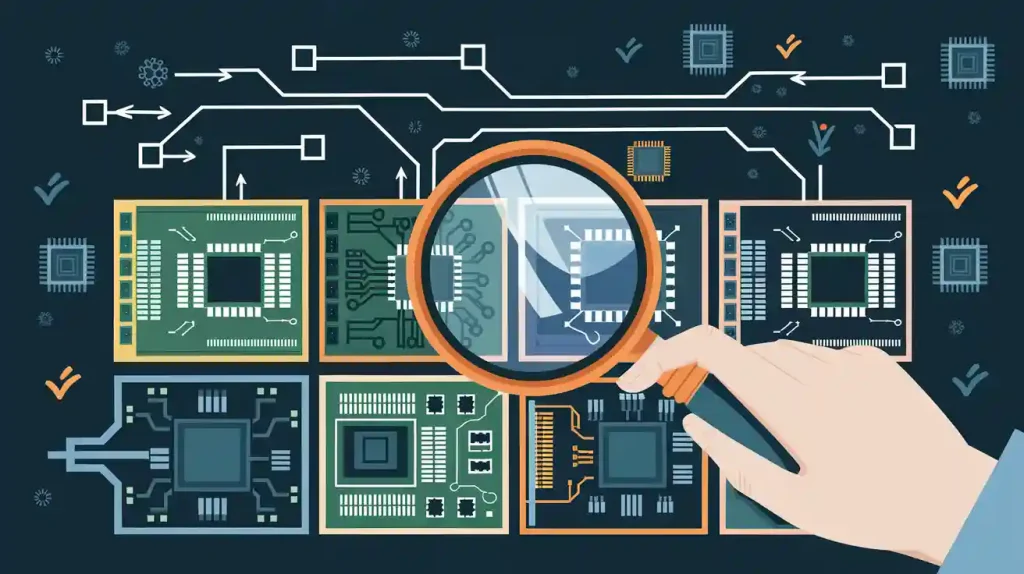
Cataloging Components
You must keep track of every part on the board. Start by making a Bill of Materials (BOM). Write down each component’s type, value, and what it does. Give each part a unique name or number. Use datasheets to help you find details about each part. If you cannot find a datasheet, try reverse engineering the pinout. You can use 3D scanning to make digital models of old parts. This helps you save the design for the future. Use tools like multimeters and analyzers to check each part. Assign a reference designator to every component. This keeps your tracing and documentation clear. When you trace the board, use these names to show how each part connects.
Removing Components (If Needed)
Sometimes you need to take parts off the board to see the traces or test them. Be careful, as removing parts can damage the board or the components. Here are some best practices:
Keep heat on the part for as little time as possible.
Use the right size desolder wick for the leads or pads.
Match your soldering iron tip to the wick width.
Cut used desolder braid often to keep it working well.
Use special tools like vacuum desoldering stations for through-hole parts.
Try hot tweezers for surface-mount devices.
Use a hot air station for small or crowded parts.
Always wear safety glasses and heat-resistant gloves.
Work in a place with good airflow.
Careful removal keeps the board safe and makes tracing easier. Always document each step with photos and notes.
Reverse Engineering Process
PCB Copy
Photographing and Scanning the PCB
You start by taking clear photos of both sides of the board. Use good lighting and a steady hand. Scanning the board with a flatbed scanner can help you see fine details. These photos help you with tracing later. If you want to reverse engineer a pcb, always keep your photos organized.
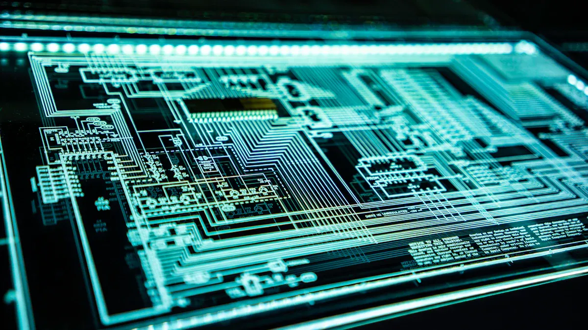
Image Correction and Trace Mapping
Next, you edit the photos to make the traces stand out. Adjust the brightness and contrast. Use image editing software to highlight pads and vias. Tracing each line on the board helps you see how signals move. Careful tracing is key for reverse engineering.
Identifying Pads, Traces, and Vias
Look closely at the board. Mark each pad, trace, and via. Use a microscope if you need to see small parts. Tracing every connection helps you understand the board’s layout. You need to check each path for breaks or damage.
Aligning and Layering Images for Double-Sided Boards
If your board has two sides, align the photos. Use software to layer the images. This helps you match traces from one side to the other. Tracing both sides lets you see the full path of each signal.
Recreating the PCB Layout in Design Software
Now, use PCB design software to draw the board. Place each component where you found it. Draw every trace and via. When you finish, you can generate Gerber files. These files are standard for making new boards. Always save your work and keep notes for each step.
BOM Remake
Cataloging and Identifying Components
You need to list every part on the board. Use your tracing and photos to match each component. Check markings and use datasheets to find details.
Researching Component Specifications
Look up each part’s value and function. Use online databases and part search engines. Tracing the circuit helps you guess unknown parts.
Creating a Bill of Materials (BOM)
Write down each part’s name, value, and where it goes on the board. This BOM helps you rebuild or repair the board.
Sourcing Replacement Parts
Find trusted suppliers for each part. Avoid counterfeit parts by checking sources. Good tracing and photos help you order the right items.
IC Unlock
Identifying Locked or Encrypted ICs
Some chips on the board may be locked. Look for markings or missing data. Tracing the pins can help you spot these ICs.
Researching Unlocking Methods
You can try software attacks, power analysis, or even special machines. Each method depends on the chip type.
Attempting to Access or Dump Firmware
If you try to unlock a chip, use the right tools. Always follow the law. Some countries have strict rules about unlocking chips.
Documenting Findings and Limitations
Write down every step you take. Keep notes on what worked and what did not. Good documentation helps others repeat your work.
Tip: Careful tracing and clear notes make pcb reverse engineering easier and safer.
Verification and Final Steps
Cross-Checking Connections
You must check that every connection matches your notes. Use a multimeter to see if pins and traces connect. This helps you find broken or missing paths. For multilayer boards, line up your pictures and trace hidden paths. Sometimes, you need to take the board apart or use special cameras to look inside. Here are some ways to check connections:
Use a multimeter to map and test traces.
Line up pictures for boards with more than one side.
Take the board apart and look with a microscope.
Use software to see if your drawing matches the real board.
Test signals with an oscilloscope to make sure they work.
Always check both easy-to-see and hidden paths. Some traces are inside the board, so go slow and check everything twice.
Testing and Troubleshooting
After checking connections, you need to test the board. First, look at the board for burnt parts or missing pads. Check for solder bridges too. Use your tools to see if power and ground are shorted. Turn on the board slowly with a power supply that limits current. Watch for problems like hot spots or lights that do not turn on.
If the board does not work, test each part by itself. Use oscilloscopes and logic analyzers to look at signals. Compare what you see to your reverse engineering drawing. If you find a problem, follow the signal path to find what is wrong. For hard boards, you might need X-ray or CT scans.
Look at the board
Check for shorts and right voltages
Test if the board works at test points
Use tools to find and fix problems
Bill of Materials and Documentation
Good notes are important for reverse engineering. Make a bill of materials (BOM) with every part on the board. Write down the part number, what it is, where to buy it, and how many you need. Take pictures before and after you take the board apart. Write down every step, including tracing and testing. Use tables and drawings to show how the board works.
Documentation Aspect | Details |
|---|---|
BOM | List part numbers, suppliers, and amounts |
Design Notes | Write down tracing and test steps |
Visual Aids | Add labeled pictures and drawings |
Test Plans | Explain how you tested the board |
Good records help you rebuild the board, save money, and make sure your work is good. Keeping clear notes makes it easier to share and do the project again.
You can get good at electronic reverse engineering if you follow each step carefully. Always write down what you do with every board. Take clear pictures and make notes for each board you work on. Use your tools to check every connection on the board. Follow these important rules to be correct and follow the law:
Ask for permission before you collect data from any board.
Only use your skills for legal board work.
Keep all board data safe with strong protection.
If you want to know more, you can try harder methods. The table below lists some ways to study boards in more detail:
Advanced Technique | Description | Example Tools |
|---|---|---|
Debugging and Disassembling | Watch how board software works and break down code. | OllyDbg, IDA Pro |
Decompilation and Code Analysis | Rebuild code from board binaries and study logic. | Hex-Rays, Binary Ninja |
Cryptography and Obfuscation | Handle encrypted or hidden board software. | x64dbg, UPX |
Malware Analysis and Forensics | Study harmful board software and investigate problems. | Wireshark, VirusTotal |
Learning and Sharing | Keep learning and share board knowledge with others. | GitHub, Reddit |
Be patient and careful with every board you work on. Keep learning new things to get better at working with boards.
FAQ
What is the first thing I should do before reverse engineering a circuit board?
First, check if you really own the board. Make sure you are allowed to work on it. Always follow the law and read any rules about reverse engineering.
Can I reverse engineer a board without removing any components?
Yes, you can usually study the board without taking off parts. Use a camera, microscope, and multimeter to look at the board. Only take off parts if you cannot see or test some traces.
What software helps with PCB reverse engineering?
You can use PCB design software like KiCad or Eagle. Image editing tools like GIMP or Photoshop help with pictures. These programs let you draw diagrams and copy the board layout.
How do I identify unknown components on a board?
Look for numbers or letters on the part.
Use a multimeter to check the pins.
Search online for datasheets.
Ask people in online forums if you need help.
Is it legal to reverse engineer any circuit board?
No, you cannot reverse engineer every board. Some designs are protected by laws. Always check copyright, patent, and contract rules before you start. If you are not sure, ask a legal expert.