In the design of electronic products, from creating the schematic to PCB layout and routing, various errors can occur due to a lack of experience or knowledge, which can hinder progress and, in severe cases, render the circuit board unusable. To prevent such issues, it is essential to improve our understanding of this area and avoid common mistakes.
This article will discuss some common drilling issues during PCB design to help you avoid repeating the same mistakes. Drilling can be categorized into three types: through-hole, blind hole, and buried hole. Through-holes include plated through holes (PTH), non-plated through holes (NPTH), and vias, all of which serve to provide electrical connectivity between layers. Regardless of the type, missing holes can lead to significant functional failures, making correct drilling design crucial.
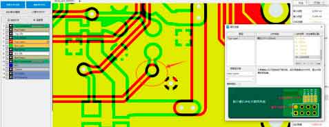
Problem 1: Slot Holes Placed on the Wrong Layer in Altium Design
- Problem Description: The slot hole was missed, rendering the product unusable.
- Cause Analysis: The designer missed creating the USB component’s slot while designing the package. When designing the board, they noticed the issue but didn’t modify the package; instead, they added the slot on the hole layer. While this approach might seem okay in theory, during manufacturing, drilling is done using the drill layers, which might cause the slot hole on other layers to be overlooked, leading to a missed hole and a non-functional product.
- How to Avoid the Pitfall: Each layer in the PCB design file has a specific function. Drill holes and slot holes must be placed in the drill layer, not just assumed to be manufacturable because they are in the design.

Problem 2: Zero-Diameter Holes in Altium Design
- Problem Description: Missing vias resulting in open circuits and non-conductivity.
- Cause Analysis: In this case, the design file had missing vias, which were flagged during the Design for Manufacturability (DFM) check. Upon further investigation in Altium, it was found that the via diameter was set to 0, making it effectively nonexistent in the design file.
- Cause: This issue arose due to an error when the designer placed the via, resulting in a zero-diameter via. If the issue isn’t detected during the DFM check, the missing vias could go unnoticed, leading to electrical open circuits and failure in functionality.
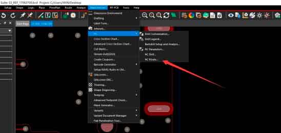
- How to Avoid the Pitfall: After completing the circuit diagram, always perform a DFM check to ensure manufacturability. Missing vias are often hard to spot, but a DFM check before manufacturing will help identify such issues.

Problem 3: Missing Via Outputs in PADS Design
- Problem Description: Missing vias result in open circuits and non-conductivity.
- Cause Analysis: During a DFM check in PADS, many missing vias were flagged. After investigating, it was found that one set of vias was mistakenly designed as semi-conductive vias, causing PADS to omit these vias from the output files. In this case, a dual-side PCB design didn’t allow semi-conductive vias, and the mistake occurred when the engineer misconfigured the vias as semi-conductive. This mistake prevented the vias from being output during the drilling process, leading to missing vias.
- How to Avoid the Pitfall: This type of error is hard to detect without a DFM analysis. Always perform a thorough DFM check after completing the design to ensure there are no issues with via outputs, especially for complex designs with different via types.


Problem 4: Missing Slot in Allegro Gerber Files
- Problem Description: Missing pin holes for HDMI components, resulting in an inability to insert the pins.
- Cause Analysis: During a DFM check, the missing slot holes were flagged. After further investigation, it was found that the Gerber file did not include the slot hole layer. This issue occurred because the drilling file was output correctly, but the slot hole layer was omitted, leading to missing slots for components like HDMI connectors. If this happens, the component pins cannot be inserted, and if the slot is for a ground network, drilling it later could cause an open ground network.
- How to Avoid the Pitfall: This type of error is common among beginners, as it’s easy to forget to output the slot hole layer. Always perform a DFM check before sending the design for manufacturing to ensure that all necessary layers, including slot holes, are included in the Gerber files.

Importance of Holes in PCB Design
The holes in PCB design are crucial for routing, structural support, and component placement. Through-holes, positioning holes, and holes for components such as DIP packages all need to be properly designed and placed. Missing holes or incorrect hole placement can result in design failure. Ensuring correct hole design and conducting thorough DFM checks are vital steps to avoid costly errors and ensure the final product works as intended.