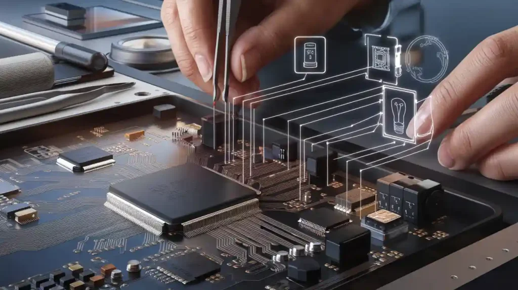
A PCB (Printed Circuit Board) is an essential electronic component, often referred to as a printed circuit or printed wiring board. The quality of the PCB largely determines the performance of electronic components, making testing a critical part of the PCB production process. Testing typically identifies functional defects, such as opens, shorts, and other issues that are not easily visible. To ensure the success of any product design, multiple rounds of testing are necessary. PCB testing helps minimize major issues, identify smaller errors, save time, and reduce overall costs.
PCB testing is mainly used to address potential problems during the manufacturing and final production stages. These tests can also be applied to prototypes or small-scale assemblies to identify potential issues with the final product.
Testing Methods for Bare PCB
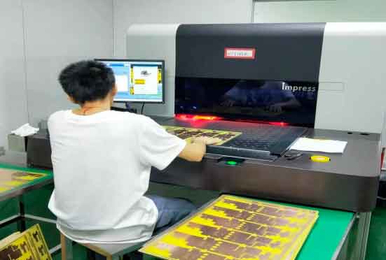
1. AOI Testing (Automatic Optical Inspection)
AOI equipment is widely used across various industries, including PCB manufacturing, as a key quality assurance tool. In the PCB production process, AOI is used to test the etched copper traces on the PCB after the pattern is created. The equipment scans the traces on the board and compares them with the design files. It then identifies any discrepancies between the board’s actual patterns and the stored data, highlighting areas of defects. The final confirmation and processing of these defects are performed by the inspector, completing the inspection process.
2. Flying Probe Testing
Flying probe testing is a highly recognized and effective test method that can effectively identify quality issues in production. It has been proven in the industry to be a cost-effective method to improve PCB standards. Flying probe testing uses two or more independent probes that operate without fixed test points. These probes are electromechanically controlled and move based on specific software instructions. As a result, flying probe testing has a low initial cost, but the testing efficiency is not as high as fixture testing since the probes test one point at a time. This method is ideal for small-batch orders.

3. Fixture Testing
A fixture is a specialized testing device designed based on the PCB layout and used for electrical performance continuity testing. It can be either single-sided or double-sided.
PCB electrical testing requires the creation of a test fixture. Metal probes in the fixture connect to the pads or test points on the PCB. When the PCB is powered, the tester measures typical values like voltage and current to determine whether the circuit under test is conducting correctly. The advantage of electrical testing is high efficiency, but the downside is its high cost, as a different test fixture is required for each PCB design. Therefore, fixture testing is suitable for large-volume orders.

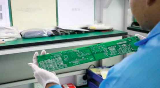
4. Manual Visual Inspection
Visual inspection is the most traditional testing method, with the advantage of low initial cost and no need for test fixtures. By using magnifying glasses or calibrated microscopes, inspectors visually check whether the PCB meets specifications and determine when corrective actions are necessary.
This method is only suitable for simple circuit boards. The main disadvantages are the possibility of human error, high long-term costs, discontinuous defect detection, and difficulty in data collection. As PCB production scales up and as trace spacing and component sizes decrease, visual inspection becomes increasingly impractical.
(PIC-Manual Visual Inspection)
PCB Test Fixture Design
For fixture testing, it is essential to design positioning holes on the PCB. Holes within the PCB should have a diameter of at least 1.5mm to serve as test positioning holes. Without positioning holes, the PCB may shift during testing, leading to inaccurate results.
Positioning holes serve as the reference points for PCB manufacturing. There are various methods for positioning holes, depending on the required accuracy. Positioning holes on a PCB should be indicated using specific graphical symbols. In cases where accuracy is not critical, larger assembly holes within the PCB can be used as substitutes.
To facilitate PCB drilling and external shape milling and to make in-circuit testing easier, many PCB manufacturers prefer designers to include four non-plated holes for positioning. These positioning holes are usually designed as non-plated, with diameters of 1.5mm or 2.0mm. If board space is tight, at least three positioning holes should be placed, typically arranged diagonally.
For panelized PCB, the entire panel can be treated as one PCB, requiring only three positioning holes, and these holes can be placed along the process edge of the panel. If the designer fails to include these holes, the PCB manufacturer will automatically add them where possible without affecting the traces, or they may use existing non-plated holes for positioning.