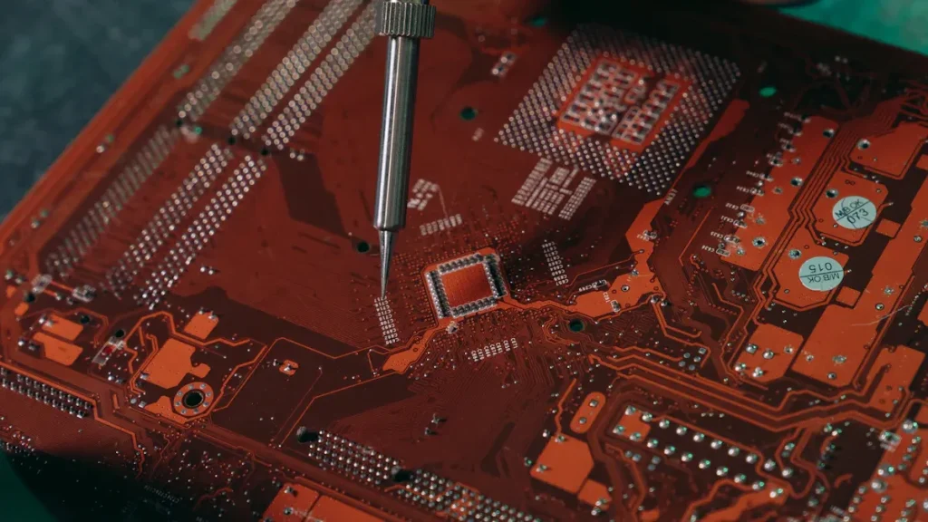
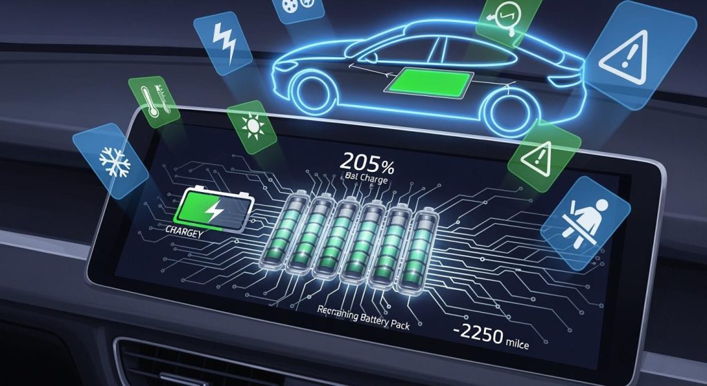
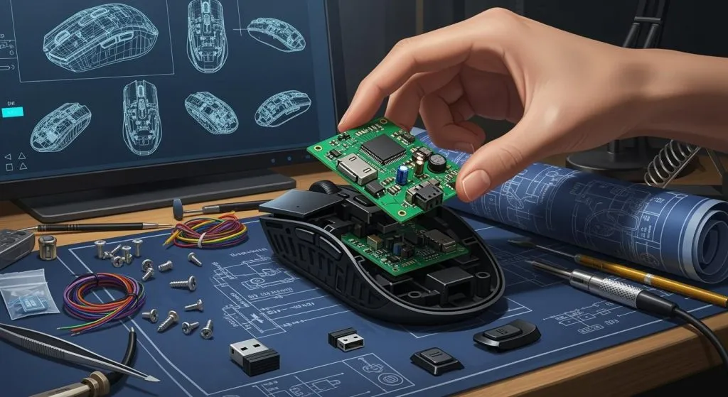
PCB stands for Printed Circuit Board, which is an important electronic component. It serves as a support for electronic components and provides electrical connections, playing a crucial role in the physical support and conduction of electronic devices. Its main function is to enable various electronic components to form circuits and electrical connections according to a pre-designed layout without damage or permanent deformation. PCB are widely used in various electronic devices, including communication equipment, computers, medical devices, and aerospace.
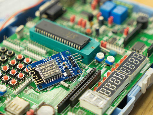
The origin of PCB can be traced back to the early 20th century when electronic devices contained many wires that tangled, occupied significant space, and often short-circuited. To solve this problem, German inventor Albert Hanssen pioneered the concept of “wiring” in the early 1900s by cutting conductive paths from metal foil and adhering them to wax paper, creating vias at intersections for electrical interconnections between different layers. This concept laid the theoretical foundation for PCB manufacturing and development.
In the 1920s, Charles Ducas from the United States proposed the idea of printing circuit patterns on insulating substrates and then electroplating to create conductors for wiring. This method opened the door to modern PCB technology. Over time, PCB technology has continuously evolved, leading to the emergence of multilayer PCB, high-precision high-density circuits, and automated production processes, making PCB indispensable in the electronics manufacturing industry.
Let’s delve into PCB production and applications!
Materials for PCB
The materials used for PCB primarily include:
- Rigid PCB materials: Commonly include phenolic paper laminates, epoxy paper laminates, polyester glass fiber laminates, and epoxy glass fabric laminates.
- Flexible PCB materials: Commonly include polyester films, polyimide films, and fluorinated ethylene propylene films.
- FR-4 (glass fiber reinforced plastic): Known for excellent insulation, heat resistance, and mechanical properties, suitable for most electronic devices.
- CEM-3 (cellulose reinforced plastic): Offers good mechanical strength and electrical performance but lower heat resistance.
- Graphene: Features outstanding conductivity, thermal conductivity, and mechanical properties, but is not widely used due to high production costs.
- Metal substrates: Provide high thermal conductivity and mechanical strength, suitable for high-power and high-frequency electronic devices.
- PTFE (polytetrafluoroethylene): Known for excellent dielectric properties and heat resistance, suitable for high-frequency electronic devices.
Additionally, other special materials can be used to manufacture PCB based on specific application needs to achieve optimal performance and cost-effectiveness.
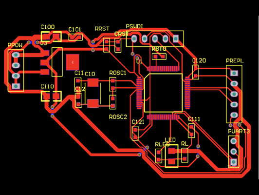
PCB Manufacturing Process
The PCB manufacturing process typically includes the following steps:
- Circuit design: Use EDA (Electronic Design Automation) software to draw the circuit diagram, considering the circuit’s functionality, component selection, and signal routing.
- Material preparation: Choose suitable substrates and copper-clad boards based on the circuit diagram’s size and requirements, and prepare all necessary components and tools.
- Circuit board production: Print the circuit diagram on the copper-clad board, followed by etching and cleaning to form the circuit board. Various methods like engraving and laser printing can be employed.
- Component soldering: Solder required components onto the circuit board, selecting appropriate soldering methods such as manual or machine soldering.
- Testing and debugging: After soldering, test and debug the circuit board to ensure proper functionality.
- Assembly and final inspection: Finally, assemble the circuit board into the product and conduct final inspections to ensure compliance with specifications.
It’s important to note that PCB manufacturing involves multiple stages and requires expertise across various disciplines. Since the quality of PCB directly impacts the overall quality and performance of electronic devices, strict quality and precision control during the manufacturing process is essential.
Types of PCB
PCB can be classified into different types according to various criteria:
By structure:
- Rigid boards: Made from inflexible, durable substrates that provide support for mounted electronic components, including fiberglass, paper, composite, ceramic, and metal substrates.
- Flexible boards: Made from flexible insulating materials, allowing for bending, rolling, and folding, accommodating space layout requirements.
- Rigid-flex boards: Combine rigid and flexible areas on a single PCB, layering flexible and rigid substrates.
- HDI boards: High Density Interconnect boards use multilayer construction and laser drilling technology for internal connections.
- Package substrates: Directly used for chip packaging, providing electrical connections, protection, support, cooling, and assembly.
By layer count:
- Single-sided boards: Only one side has conductive patterns.
- Double-sided boards: Both sides have conductive patterns.
- Multilayer boards: Composed of alternating layers of conductive patterns and insulating materials.
By application area: Divided into communication, consumer electronics, computer, automotive electronics, military/aerospace, and industrial control boards.
By specific end-product application: Mobile phone boards, television boards, audio equipment boards, electronic toy boards, camera boards, and LED boards.
PCB Industry Development Stages
The global PCB industry has gone through several stages:
- Demand from household appliances and communication devices (1980-1991): The proliferation of household appliances and communication electronics propelled industry growth.
- Desktop computer penetration and industry upgrade (1992-2000): The rise of desktop computers expanded PCB demand, prompting technology upgrades.
- Growth due to smartphones, laptops, and communication upgrades (2001-2018): Advances in communication technology and the spread of smart devices continued to drive PCB demand.
- Current growth cycle: The industry is experiencing new growth driven by 5G communication technology, automotive intelligence and electrification, cloud computing, and the Internet of Things.
Future Directions in the PCB Industry
- High density, miniaturization, and thinness: As electronic devices trend toward smaller, lighter designs, PCB must meet increased density and compactness requirements, driving advancements in manufacturing technology.
- Environmental sustainability: The industry is actively promoting environmentally friendly production, adopting lead-free and halogen-free materials, and developing recycling technologies for discarded PCB.
- Application of new materials: The emergence of new materials like carbon nanotubes and graphene provides opportunities for higher performance and miniaturization in PCB.
- Intelligent and integrated designs: The development of IoT and AI drives PCB toward intelligent and integrated designs, such as smart sensor PCB combining sensors and data processing units.
- Customization and small-batch production: The increasing variety and personalization of electronic devices require more flexible and efficient PCB production processes.
The PCB industry’s future is closely linked to electronic device advancements, with steady growth anticipated. As technology progresses and application areas expand, the PCB industry will encounter more opportunities and challenges.
Challenges in High-Density PCB Development
- Signal integrity: Increased line density can lead to interference and noise during signal transmission, causing issues like signal delay and distortion.
- Power integrity: Managing power distribution and noise on high-density PCB presents significant challenges for overall system stability.
- Thermal management: Compact component arrangements necessitate effective heat dissipation strategies to prevent overheating.
- Manufacturing process: Higher precision and stricter control are required for high-density PCB manufacturing, increasing complexity and costs.
- Cost: As technology advances and component density increases, manufacturing costs rise, necessitating cost reduction strategies without compromising performance.
- Design complexity: Designing high-density PCB requires a higher level of expertise, and maintaining skilled design teams is a challenge.
Influencing Factors for PCB Industry Outlook
- Technological advancements: Continuous evolution in technology presents opportunities for the PCB industry as device complexity increases.
- Emerging application fields: New domains such as IoT, smart home, and intelligent manufacturing will generate new growth for the PCB industry.
- Environmental and sustainability considerations: Heightened global focus on environmental issues will prompt PCB industries to comply with stricter regulations and develop more eco-friendly materials and processes.
- Market competition: Despite ample market opportunities, intense competition requires firms to enhance quality and reduce costs.
To address these challenges, PCB manufacturers and designers need to explore new technologies and materials, improve manufacturing accuracy and reliability, enhance thermal and power management, reduce costs, and optimize design workflows. Additionally, the industry must focus on talent development and technological exchange to foster innovation and progress.
Overall, the outlook for the PCB industry is optimistic. With ongoing technological advancements, the increasing application of electronic devices across various fields will sustain demand for PCB. Notably, the proliferation of 5G, IoT, and AI will usher in further opportunities for growth in the PCB industry.