There are many safety distance considerations in PCB design, including spacing between traces, character spacing, pad spacing, and more. Here, we classify them into two categories: electrical-related safety distances and non-electrical-related safety distances.
01 Electrical-Related Safety Distances
Trace-to-Trace Spacing
For the processing capabilities of mainstream PCB manufacturers, the minimum distance between traces should not be less than 0.075mm. The minimum trace spacing refers to the smallest distance between a trace and another trace or between a trace and a pad. From a manufacturing perspective, larger trace spacing is better. A more common value is 0.127mm.
Pad Hole Diameter and Pad Width
For mainstream PCB manufacturers, if the pad uses mechanical drilling, the minimum hole diameter should not be less than 0.2mm. If laser drilling is used, the minimum hole diameter should not be less than 0.1mm. The hole diameter tolerance may vary slightly depending on the material, but it is generally controlled within 0.05mm. The minimum pad width should not be less than 0.2mm.
Pad-to-Pad Spacing
For mainstream PCB manufacturers, the minimum distance between pads should not be less than 0.2mm.
Copper-to-Edge Spacing
The minimum distance between live copper and the edge of the PCB should ideally not be less than 0.3mm. This can be set in the Design Rules > Board Outline page.
For large-area copper pours, it is common to reduce the copper area inward from the board edge, typically set at 0.2mm. In the PCB design and manufacturing industry, to avoid potential issues like copper exposure at the board edge causing warping or electrical shorts, engineers often reduce the copper area inward by 8 mils rather than extending it all the way to the edge.
There are many ways to achieve this copper offset, such as drawing a keep-out layer at the board edge and setting the distance between the copper pour and the keep-out area. A simpler method is to set different safety distances for the copper objects, such as setting the overall board safety distance to 0.25mm and the copper pour distance to 0.5mm, which will result in a 0.5mm offset from the board edge while eliminating potential dead copper areas in components.
02 Non-Electrical-Related Safety Distances
Character Width, Height, and Spacing
In the case of silkscreen processing, no modifications should be made to the font. Any characters with a line width (D-CODE) less than 0.22mm (8.66 mils) should have their lines thickened to 0.22mm. The overall character width (W) should be 1.0mm, and the character height (H) should be 1.2mm. The spacing between characters (D) should be at least 0.2mm. If the characters are smaller than these specifications, they will appear blurry when printed.
Via-to-Via Spacing
The spacing between vias (via-to-via, center to center) should be at least 8 mils.
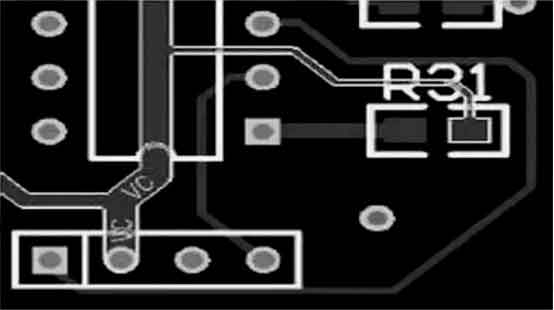
Silkscreen to Pad Spacing
The silkscreen should not overlap the pads. If the silkscreen covers a pad, it will prevent the pad from being properly soldered during the assembly process. A recommended clearance is at least 8 mils. If the PCB area is limited, a 4 mil clearance may be acceptable, but this should be avoided if possible. If the silkscreen inadvertently overlaps the pad during design, the manufacturer will usually remove the silkscreen in the pad area to ensure proper soldering.
In some cases, designers may deliberately place the silkscreen close to the pads, particularly when two pads are very close together. In such cases, the silkscreen can effectively prevent short circuits between soldering pads, but this needs to be considered on a case-by-case basis.
Mechanical 3D Height and Horizontal Spacing
When placing components on the PCB, it’s essential to consider whether they will conflict with other mechanical structures in terms of both height and horizontal spacing. During the design phase, it’s important to ensure there is adequate spacing between components, the PCB and the product’s outer shell, and other structural elements to avoid physical conflicts. Proper clearance must be provided to ensure no interference occurs.
The above values are for reference and can provide direction when defining safety margins in your designs, but they do not represent strict industry standards. Specific requirements may vary depending on the PCB manufacturer or the product’s design constraints.