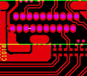
The production of single-sided or double-sided PCBs typically involves drilling non-conductive or conductive holes directly after the material is cut, while multi-layer boards are drilled after the lamination process. Holes are categorized based on their function, including component holes, tool holes, through holes (Vias), blind holes, and buried holes (blind and buried holes are a type of via hole). Conventional drilling is done using mechanical drilling equipment. In actual manufacturing, the spacing between holes usually impacts both the machining process and the final product’s reliability.
Hole Spacing Manufacturing Requirements:
Via Holes (Conductive Holes):
- Minimum Hole Diameter: Mechanical drilling 0.15mm, laser drilling 0.075mm.
- Pad to Board Edge Spacing: 0.2mm.
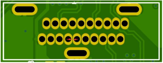
- Via Hole to Via Hole Spacing (Edge to Edge): Cannot be less than 6 mil; preferably greater than 8 mil. This is very important and must be considered during design.
- The minimum via hole diameter is typically no smaller than 0.2mm, and the pad single-side distance should not be less than 4 mil, preferably greater than 6 mil, with no upper limit. This is very important and should be considered.
Pad Holes (PTH):
- Pad to Board Edge Spacing: 0.25mm.
- The size of the pad hole is determined by the component used, but it should be at least 0.2mm larger than the component pin. For instance, a component with a 0.6mm pin should have a hole of at least 0.8mm to avoid difficulties due to manufacturing tolerances.
- Pad Hole to Pad Hole Spacing (Edge to Edge): Cannot be less than 0.3mm. The larger, the better. This is critical and must be considered.
Non-Plated Holes and Slots (NPTH):
- Non-Plated Slot Hole Spacing: The minimum spacing should be at least 1.6mm, or it could cause an increased risk of broken holes and difficulty in edge milling.
- The distance from non-plated slots to the board edge should not be less than 2.0mm to avoid broken holes. Longer slots should have a greater distance from the board edge to prevent separation at the edge.
- Non-Plated Stamped Holes: For connecting boards together, these holes should be spaced not too small or too large to avoid breaking the board. The recommended spacing is typically between 0.2-0.3mm.
Reliability Impact of Hole Spacing:
Hole-to-Hole Spacing:
This refers to the distance from the inner wall of one hole to the inner wall of another, not the distance between the pads. It’s crucial to distinguish between these measurements.
If the hole-to-hole spacing is too small, what are the potential issues?
- If holes within the same network are too close, they can cause broken holes, burrs, and other defects that impact the appearance and assembly.
- For holes in different networks, insufficient spacing could cause broken holes, burrs, or even short circuits due to the capillary effect.
Capillary Effect (Chip Sucking Effect): The capillary effect occurs due to the high-speed rotation of the drill bit and the pressure it exerts on the surrounding PCB material. This can loosen the fiberglass inside the board, leading to issues such as poor hole formation and short circuits when the copper plating penetrates these loose areas.
According to IPC-A-600G guidelines:
For the capillary effect, B should not reduce the trace spacing below the minimum required by procurement specifications, and A should not exceed 80mm (3.150in). The same applies to hole spacing.
Another negative effect caused by tight hole spacing is the CAF (Conductive Anodic Filamentation) effect:
- CAF Effect: It refers to copper ions migrating along microcracks in the resin or fiberglass between conductors under high voltage and temperature conditions, leading to leakage currents.
- This occurs when the PCB/PCBA operates in high-temperature and high-humidity environments, resulting in poor insulation between conductors and eventual short circuits. CAF typically happens between vias, or between vias and traces, or between outer traces, reducing insulation and leading to failure.
Hole Spacing Manufacturability Checks:
1. Same Network Vias: If two vias are too close during drilling, the PCB’s drilling efficiency could be compromised. After drilling the first hole, the material between holes could become too thin, resulting in uneven forces on the drill bit, inconsistent cooling, and drill bit breakage. This leads to poor hole formation or unconnected vias.
2. Different Network Vias: Every layer in a PCB requires a via pad with specific surrounding environment conditions, including whether traces are adjacent or not. If the spacing is insufficient, some via pads might lose their copper connection, potentially causing shorts. To avoid this, a 3 mil safety distance between different network vias is essential.
3. Different Network Component Holes: Minor alignment offsets during production can affect the spacing between component holes from different networks. In these cases, the safety distance is ensured by trimming the pad. This trimming may lead to irregular shapes or, in the worst case, cause the hole to break or create a short circuit during soldering.
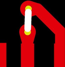
4. Blind and Buried Vias:
- Blind Vias: These are vias that connect internal layers to the outer layers but do not pass through the entire PCB.
- Buried Vias: These connect internal layers only and are invisible from the surface of the PCB.

When the spacing between blind and buried vias is too small or nonexistent, it results in a “stacked hole.” The design may face manufacturing difficulties, especially when the vias location does not allow for proper connection. In such cases, a special process is required to ensure the vias are electrically connected after drilling. This involves completing the buried via drilling before plating and then drilling the blind vias.