PCB design is a complex process that involves various unforeseen factors that can impact the overall outcome. To ensure high-quality PCB production on time—without extending design time or incurring costly rework—design and circuit integrity issues must be identified early in the process.
However, there are many minor details in PCB design that, if overlooked, can significantly affect the PCB’s performance and even determine the product’s success or failure. To maximize design efficiency and product quality, what additional details should we focus on?
Through practical experience working with customers, we’ve summarized key considerations for silkscreen, outline, and panelization design. As a high-reliability multilayer PCB manufacturer, Wonderful PCB specializes in PCB R&D and manufacturing, delivering high-reliability and fast-turnaround prototyping experiences. Our mission, “Lower Costs and Improve Efficiency for the Electronics Industry,” reflects our understanding that design development and engineering costs, while a small percentage of the production chain, can have a significant impact on total costs.
Considering the crucial role of the design phase in final product quality and cost, we share expert solutions to real-world cases involving silkscreen, outline, and panelization design issues to support cost-effective and efficient full-process manufacturing.
Silkscreen Design Case

Case 1: Standardizing Silkscreen Design
Issue:
Industry standards for surface-mount devices do not have stringent requirements for silkscreen labeling. However, from an engineering perspective, labeling over open solder pads is treated as a design anomaly, leading to back-and-forth communication (EQ) and time delays.
Expert Recommendation:
To facilitate repair and soldering, place reference designators outside the component boundary. In dense areas, arrange reference designators sequentially or omit them entirely if necessary.


Outline Design Cases
Case 1: Inner Slot Design with Consideration for Milling Feasibility and Production Efficiency
Issue:
The customer provided a design file where the inner slot needed to be hollowed out, but the spacing at the curved section was less than 0.8mm, preventing the use of a standard milling tool.
Expert Recommendation:
If it does not affect the board’s functionality, suggest increasing the spacing at the curved sections. For sharp corners, add “relief holes” (see white arrow in the image) to facilitate milling.

Case 2: Board Edge Connection Design
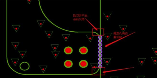
Issue:
For a design with adjacent boards, one side has rounded edges, and the other has straight edges connected by perforations (mouse bites). When milling, sharp edges are caused after depaneling, which must be filed into rounded edges during post-soldering processes. For perforations, drilling at both ends can slightly damage the board, potentially causing disputes despite adherence to PCB standards.
Expert Recommendation:
Where structural integrity allows, change the rounded edge to a straight edge or add “relief holes” to enhance production efficiency and produce aesthetically superior boards.

Panelization Design Case
Case 1: Panelization Orientation

Issue:
When customers provide panelization diagrams that are perfectly symmetrical (left image) or physical reference images (right image) without clearly marking panelization orientation, it becomes challenging for downstream personnel to identify the correct orientation. Misinterpretation as aligned panelization can lead to interference issues during soldering, making assembly impossible.
Expert Recommendation:
From a standards perspective, the design file must include explicit orientation markers (except in non-symmetrical designs).


Conclusion
The cases above demonstrate several details of optimizing PCB design. As a digital service platform dedicated to improving traditional electronics industry workflows, Wonderful PCB has addressed these real-world cases during the order fulfillment process.
We uphold our promise to global customers with high-reliability products, transparent delivery experiences, and trustworthy services. Through continuous improvement, we remain committed to our mission: “Lower Costs and Improve Efficiency for the Electronics Industry.”