Vias are an unavoidable aspect of PCB design. During the layout process, avoiding all crossover lines is often challenging. To resolve this, vias are used to achieve interlayer connectivity, leading to the development of double-sided and multilayer PCBs. Consequently, vias have become a critical element of PCB design.
From a design perspective, vias serve two main purposes: electrical connection and mechanical support or positioning. These roles fulfill electrical requirements or physical needs. Therefore, vias are often classified further into electrical vias and mechanical support holes, with the latter divided into solder pad holes (typically plated) and mounting holes (often non-plated).
A via mainly consists of two parts:
- Drill hole: The central hole.
Pad area: The area surrounding the drill hole.
- The sizes of these two components determine the overall via size.
In high-speed, high-density PCB designs, designers typically aim for the smallest possible vias to maximize routing space and minimize parasitic capacitance, making them more suitable for high-speed circuits. However, reducing via size increases manufacturing costs and faces technical constraints:
- Smaller holes require longer drilling times and are prone to center misalignment.
- When the hole depth exceeds six times the drill diameter, uniform copper plating on the hole walls becomes difficult.
Balancing design and production involves numerous considerations. While some designs can be directly sent to production, others require additional engineering checks to address potential issues, avoiding delays, yield problems, and reliability concerns.
Given the significant impact of design decisions on overall costs and schedules, these challenges are preventable. As a high-reliability multilayer PCB manufacturer, Wonderful PCB focuses on PCB R&D and manufacturing, delivering fast-turnaround, high-reliability PCBs. Our mission, “Lower Costs and Improve Efficiency for the Electronics Industry,” underscores the importance of early-stage design considerations. Below are expert solutions for optimizing hole and slot designs based on real-world cases to support efficient and cost-effective manufacturing.
Hole Design Cases
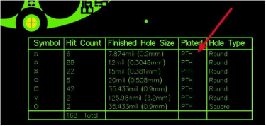
Case 1: Standardizing PTH/NPTH Design

Issues:
- As shown in the left diagram, pads are designed with electrical connections but are implemented as non-plated holes.
- As shown in the right diagram, pads are designed without electrical connections but are implemented as plated holes.
Expert Recommendations:
- For Non-Plated Holes: Ensure no electrical connections to the corresponding pads. The pad and hole size should match, or no pad should be designed.
- For Plated Holes: Ensure electrical connections to the corresponding pads, with the pad size approximately 5 mils larger than the hole diameter.
Avoid designing plated holes with no pads, as this requires positive plating processes, which extend lead times by at least a day.
Correct Design:

(Left non-metallic hole, Right metallic hole)
- Provide a hole table clearly distinguishing plated from non-plated holes to reduce EQ communication and potential design misunderstandings.
Correct Design:
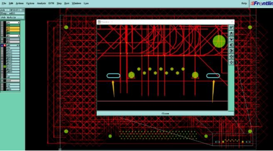
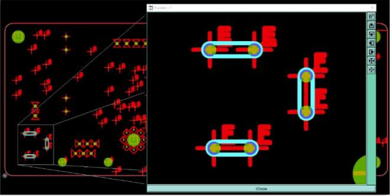
Case 2: Differentiating Metal and Non-Metal Slots

Issues:
- A design includes seven slots, with three intended as non-metal and four as metal slots. However, all slots are placed in the same GDD layer, which defaults to non-metal slots. To prevent exposed copper during milling, the plating pads are removed for non-metal slots.
Expert Recommendations:
- Separate non-metal slots into the GDD or GM1 layer and metal slots into the DRL layer or a dedicated Slot layer.
Correct Design:

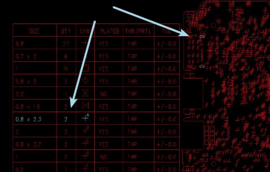
Case 3: Clear and Consistent Hole Annotations
Issues:
- Overly large hole symbols make it difficult to match holes to their symbols, causing challenges in identifying mismatched hole positions or sizes.
- Slots are hidden in corner annotations or absent from the hole table, increasing the risk of omission.
Expert Recommendations:
- Use appropriately sized hole symbols for one-to-one matching with drill holes.
- Include a hole table marking slot positions and parameters, or integrate slots directly into the DRL layer.
Correct Design:
Case 4: Avoid Conflicts Between Holes and Slots
Issues:
- The same position is used for both a hole and a slot without clear instructions.
Expert Recommendations:
- Do not design both a hole and a slot at the same location.
- Provide a hole table marking slot positions and parameters, and place slots directly in the DRL layer.
Correct Design:

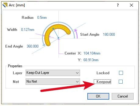
Case 5: Prevent Locked Slots in PCB Files
(pic-PCB Manufacturability Holes and Slots-9)
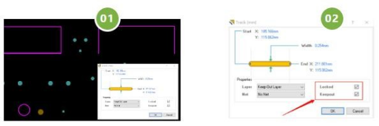
Issues:
- Slots may be “locked” during PCB-to-Gerber file conversion, resulting in missing slot designs.
Expert Recommendations:
- For designs using Altium Designer 16 or earlier, unlock slot designs before file conversion to ensure slot data is included.
Correct Design:
Case 6: Solder Mask Via Filling Tolerance Should Not Exceed 0.2mm
Issue:
- Large variations in solder mask filling tolerance result in underfilled large vias or excessive solder mask overflow in small vias.
Expert Recommendation:
- When designing vias with solder mask filling, ensure the tolerance does not exceed 0.2mm.
Correct Design:
Via(max) – Via(min) ≤ 0.2mm
Conclusion
These six cases illustrate the importance of applying best practices and following standard steps during the design phase to save time, prevent issues, and ensure higher yields and faster production.
As a digital service platform committed to improving traditional electronics industry workflows, Wonderful PCB has resolved these real-world cases during customer engagements. By delivering high-reliability products, transparent delivery experiences, and trustworthy services, we uphold our promise to global clients, fulfilling our mission: “Lower Costs and Improve Efficiency for the Electronics Industry.”