When a PCB engineer lays out a product, it involves more than just component placement and routing. Designing the power and ground planes in the inner layers is equally critical. Managing inner layers requires consideration of power integrity, signal integrity, electromagnetic compatibility, and Design for Manufacturability.
Difference Between Inner Layers and Outer Layers
Outer layers are used for routing and soldering components, while inner layers are dedicated to power and ground planes. These layers are only present in multilayer boards, where they provide pathways for power and ground. Common designs, such as double-layer, four-layer, and six-layer boards, refer to the number of signal layers and internal power/ground layers.
Inner Layer Design
1. Ground Layer Under Critical Signals
For high-speed, clock, and high-frequency signals, placing a ground layer directly beneath these signals minimizes loop path length and reduces radiation.
2. Power Plane and Ground Plane Area
In high-speed circuit design, power plane radiation and system interference must be minimized. Typically, the power plane area should be smaller than the ground plane to allow the ground plane to shield the power plane. A common rule is to shrink the power plane inward by twice the dielectric thickness compared to the ground plane.
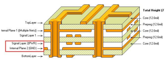
3. Layer Stacking Plan
Power planes should be adjacent to their corresponding ground planes to form coupling capacitance. This, combined with decoupling capacitors, reduces power plane impedance and provides effective filtering.
4. Reference Plane Selection
The choice of a reference plane is crucial. While power and ground planes can both act as references, the ground plane generally offers superior shielding as it is typically grounded. Ground planes are preferred as reference planes.
5. Avoid Cross-Area Routing
Critical signals in adjacent layers must not cross-segmented areas. Cross-segmentation can create large signal loops, resulting in significant radiation and coupling.

6. Power and Ground Routing
Maintain the integrity of the ground plane. Avoid routing signal lines through it. If the signal density is high, consider routing along the edges of the power plane.

Inner Layer Manufacturing
The manufacturing process for inner layers is just one part of the complex PCB fabrication workflow. Inner layer production must account for other steps in the process, such as lamination and drilling tolerances, which can affect quality and yield. Multilayer PCBs, in particular, require more intricate processes compared to single- or double-layer boards. Designers must consider these complexities during the design phase.
1. Remove Non-Functional Pads (NFPs)
Non-functional pads (NFPs) are pads in the inner layers that are not connected to any network. During PCB manufacturing, NFPs are removed because they do not impact the product’s functionality but can affect quality and production efficiency.
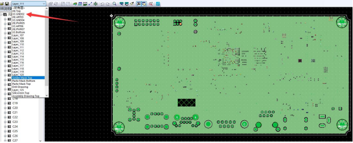
(PIC-PCB Inner Layer-4)

2. Handle Dense Vias in BGA Areas
BGA devices often have small footprints with densely packed pins, leading to dense via fan-outs. During manufacturing, vias must maintain a safe distance from traces and copper areas to prevent short circuits during lamination and drilling. If the copper between vias cannot be retained, it can cause open circuits in the network. CAM engineers must address this by adding copper bridges between vias to ensure network connectivity.
3. Address Inner Layer Design Anomalies
In inner layer designs using negative films, if all vias are fully isolated from the copper, no functional connection is achieved. Such designs render the inner layer ineffective. Manufacturers will confirm with designers to verify whether the design is intentional or if the copper has not been assigned to a network.

4. Negative Film Bottlenecks in Inner Layers
During the division of power and ground planes in inner layers, dense vias can create bottlenecks in network conductivity. If the copper bridge connecting power networks is too narrow, it cannot carry sufficient current, leading to potential board failure. In severe cases, bottlenecks may cause open circuits, resulting in design failure.

By addressing these considerations, PCB engineers can enhance the manufacturability and reliability of inner layers while avoiding design pitfalls during fabrication.