You might hear solder mask called different names in electronics. The table below shows some common names:
Alternative Name | Description |
|---|---|
Solder mask | A thin layer like paint put on PCBs. |
Solder stop mask | Another name for solder mask. |
Solder resist | Means the same as solder mask. |
Coverlay | Used for boards that can bend. |
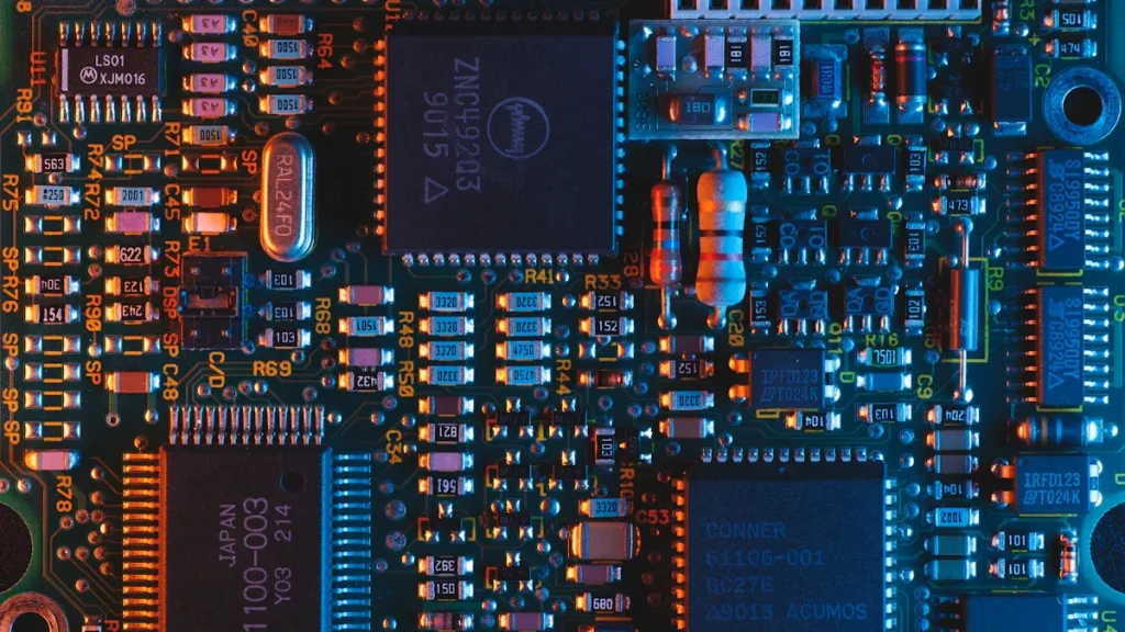
Solder mask covers copper lines on your circuit board. It helps protect copper and stops solder from making bridges. This layer makes your board work better by stopping rust and harm. Studies show solder mask stops electrical shorts and keeps your board safe for a long time.
Key Takeaways
Solder mask keeps copper traces safe on PCBs. It stops damage and rust. This helps the PCB work well.
Solder mask lowers the chance of solder bridges. Solder bridges can make short circuits. They also cause mistakes when putting parts together.
There are different solder mask types. Liquid Photoimageable and Dry Film are two examples. Each type has its own good points. Some cost less, some are faster to use, and some last longer.
Picking the right solder mask thickness is very important. It helps keep signals strong. It also stops problems in high-frequency designs.
Solder mask comes in many colors. Each color has a special use. Some colors cut down noise. Others make it easier to see during checks.
Solder Mask Overview
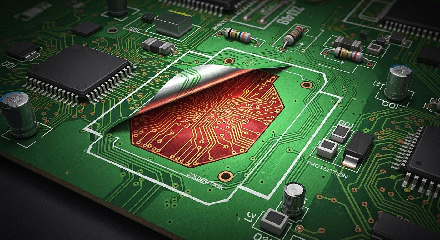
What Is Solder Mask
A solder mask layer is a thin coat on copper traces. This layer works like a shield for the copper. It keeps copper safe from harm and stops solder from spreading. Different materials are used to make this layer. The table below lists the main types used in PCB making:
Solder Mask Type | Description |
|---|---|
Epoxy Liquid | This is the cheapest type and is put on with a silkscreen. |
Liquid Photo-Imageable Solder Mask | This ink can be sprayed or silkscreened, then needs light and development. |
Dry-Film Photo-Imageable Solder Mask | This type uses vacuum lamination before light and development for exact copper layers. |
Most boards use green solder mask, but white and black are also common. Every PCB needs a solder mask, no matter how simple or advanced.
Key Functions and Benefits
Solder mask does more than just look nice. It gives your board many important benefits:
Stops solder bridges between close pads, which is very important for crowded designs.
Acts as a wall to block unwanted solder connections.
Protects copper from rust and damage, so your board works well.
Stands up to strong chemicals and high heat during soldering and cleaning.
Gives strong electrical insulation, often over 500V per mil.
Stays tough and resists damage, so your board lasts longer.
Sticks tightly to the board, so it does not peel or crack.
Tip: If you skip solder mask in crowded PCB designs, you get more solder bridges, less accuracy, and lower reliability.
The table below shows the chemical properties that make solder mask work well:
Property | Description |
|---|---|
Chemical Resistance | Stands up to strong chemicals used in soldering and cleaning, so it does not break down. |
Thermal Stability | Handles high heat during soldering, usually up to 260°C for short times. |
Electrical Insulation | Gives strong insulation, often over 500V per mil. |
Durability | Resists damage, keeping the board strong for a long time. |
Adhesion | Sticks well to the board and copper, so it does not peel or crack. |
Solder mask also protects against fire and water. It stands up to solvents and keeps its color even with heat.
Why Solder Mask Matters in PCB Manufacturing
Using a solder mask layer helps you make more good boards. The mask stops solder bridges, which can cause shorts and broken devices. It helps solder stick only to the right spots, so there are fewer mistakes. A good solder mask can cut assembly mistakes by up to 90%.
Solder mask stops short circuits and keeps copper from rusting.
It helps solder go to the right places, making assembly better.
The mask helps control heat and makes light reflect better, which is important for LED boards.
If you do not use solder mask in crowded designs, you get more problems. You will see more solder bridges, less accuracy, and lower reliability. Experts say solder mask is one of the best ways to protect PCBs.
Types and Colors of Solder Mask

Liquid Photoimageable (LPI)
Liquid Photoimageable solder mask is used in most PCB factories. This type uses a liquid that gets hard when UV light hits it. You can put it on fast, often in under 30 minutes. LPI costs less, about 20-30% cheaper than other choices. The layer can be 0.5 to 1.5 mils thick. It gives okay detail, about 4-5 mils, which is fine for normal boards. LPI can crack or peel if the board gets stressed, so think about where you will use your board.
Property | Liquid Photoimageable (LPI) | Other Types (e.g., Dry Film) |
|---|---|---|
Cost-Effectiveness | Lower | Higher |
Application Speed | Faster | Slower |
Thickness Consistency | Varies | More consistent |
Resolution | Moderate | Higher |
Durability | Less durable | More durable |
Dry Film and Peelable Types
Dry film solder mask uses a special layer that reacts to light. You put it on with vacuum lamination. This makes the thickness even and the details sharper. Peelable solder mask protects some spots during wave soldering and plating. You can use it to cover gold fingers and connectors from solder and chemicals.
Protects during wave soldering
Masks for special plating and surface work
Keeps soldered spots safe in many reflow steps
Shields gold fingers and connectors
Solder Mask Colors and Their Uses
You can pick from many solder mask colors. Green is most popular because it shows copper and silkscreen clearly. Blue is good for high-frequency boards and lowers noise. Red is easy to see for checking boards. Yellow is bright and helps with prototypes. Black looks cool and cuts down on electromagnetic signals. White bounces light, so it works well for LED boards. Purple stands out and is good for branding.
Color | Advantages | Disadvantages |
|---|---|---|
Green | Easy to see, cheap, found everywhere | Not special |
Blue | Lowers noise, good for high-frequency | Costs more, not common |
Red | Easy to check, good for inspection | Costs more, not common |
Yellow | Bright, good for prototypes | Harder to see, not found much |
Black | Looks cool, lowers signals | Hard to see, costs more |
White | Bounces light, looks clean | Gets dirty, hard to see |
Purple | Stands out, good for branding | Hard to find, costs more |
Solder Mask Application Process
Application Steps
You need to follow a careful process to apply the solder mask layer during PCB manufacturing. Each step helps you get a strong and reliable finish. Here are the main steps:
Clean the PCB surface. Remove dust and oil so the solder mask sticks well.
Apply the solder mask material. Use screen printing, spraying, or lamination.
Define the pattern. Place a photomask over the board and shine UV light to mark where the solder mask should stay.
Cure the solder mask. Use heat or UV light to harden the layer.
Inspect and check quality. Look for bubbles, peeling, or missed spots.
Tip: Careful cleaning and inspection help you avoid common defects like bubbles, poor adhesion, or scratches.
Negative Output and Exposed Pads
You want the solder to stick only to the right places. The negative output process helps you do this. It keeps the pads uncovered during solder mask application. This process maps the solder mask so only the copper pads stay exposed. You get better solder joints because the mask does not cover the pads. This step is very important for preventing solder defects and making sure your board works well.
The negative output process leaves pads open for soldering.
It helps you avoid covering copper pads with the solder mask layer.
You get precise mapping, so solder only goes where you want.
DFM Guidelines for Solder Mask
Design for Manufacturability (DFM) helps you make better boards. Follow these guidelines to optimize your solder mask design:
Make sure the solder mask covers enough area and leaves a gap of 0.1 to 0.15 mm around pads. This stops solder bridges.
Pick the right solder mask type. Use NSMD pads for fine-pitch parts and tent vias to stop solder from flowing away.
Keep the solder mask thickness between 0.01 mm and 0.03 mm. Liquid photoimageable masks work best for complex boards.
Remove solder mask from heat sinks and keep pad-to-pad bridges at least 4 mils wide.
Check your design with your PCB maker. Make sure your files match their rules.
Solder Mask Standards and Thickness
Industry Standards (IPC, UL)
You must follow special rules when using solder mask on circuit boards. These rules help your board stay safe and work well. Two main groups make these rules: IPC and UL. IPC rules tell you how to put on and test solder mask. UL rules check for safety, like stopping fires.
Here is a table with the most important IPC rules for solder mask:
Standard | Focus Area |
|---|---|
IPC-SM-840 | Sets rules for how solder mask should work and last. |
IPC-6012 | Sets rules for how strong and good rigid PCBs must be. |
IPC-A-600 | Sets rules for how PCBs should look and what is okay, including solder mask. |
You should ask your PCB maker which rules they use. This helps you avoid problems when making your board.
Typical Thickness Ranges
The thickness of solder mask is very important for your board. The right thickness protects copper and keeps solder in place. If it is too thick or thin, your board may not work right.
Most boards use solder mask that is 0.8 to 1.5 mils thick (20 to 38 micrometers). The table below shows the usual thickness:
Application Type | Thickness Range (mils) | Thickness Range (micrometers) |
|---|---|---|
General Use | 0.8 – 1.5 | 20 – 38 |
Some areas need different thickness:
Over circuit lines: about 0.5 mils or more
Over bends in circuits: about 0.3 mils
Screen printed masks are thicker than spray ones
Solder mask thickness changes how signals move on your board. A thick layer can make capacitance go up and impedance go down. A thin layer can make impedance go up. If thickness changes too much, signals may not work right, especially in fast circuits.
Tip: Always ask your PCB supplier about the best solder mask thickness for your board. This helps your board work better and last longer.
Role of Solder Mask in PCB
Electrical Insulation and Short Circuit Prevention
Every pcb manufacturing process needs strong electrical insulation. The solder mask layer works like a shield between copper traces. This shield stops short circuits, especially when traces are close together. Solder mask keeps solder from making unwanted bridges. It protects copper from oxidation and keeps your board safe. Solder mask film can handle 40-100 volts per micron. This helps your design stay reliable.
It insulates copper traces to stop shorts.
It shields copper from oxidation and dirt.
It stops solder bridges during assembly.
Facilitating Precise Soldering
You want soldering to be accurate for small parts. Solder mask design helps control where solder goes. Liquid Photoimageable solder mask makes exact openings for pads. Solder mask defined pads keep solder in the right place. The mask opening is smaller than the pad, so solder does not spread too much. This control lowers the risk of solder bridges and helps assembly yield.
Solder mask size matches pad layout for accuracy.
Solder mask layer keeps solder on the right spots.
Protection Against Environmental Factors
Your board faces many risks from the environment. Solder mask layer protects against heat, chemicals, and UV light. Here are common threats and how solder mask helps:
Environmental Factor | Description |
|---|---|
Thermal Stress | Too much heat can change the color. |
Chemical Exposure | Cleaning agents and flux can react with the mask. |
UV Exposure | Sunlight can change the mask color. |
Manufacturing Issues | Bad curing or dirt can hurt the mask. |
Material Incompatibility | Wrong materials can cause problems. |
Mitigation Measures | Use UV-resistant mask, good packaging, and conformal coating. |
Enhancing Signal Integrity and Board Longevity
You need stable signals for high-frequency designs. Solder mask thickness affects signal quality and impedance. A uniform solder mask film blocks crosstalk and interference. If thickness changes, you may see signal loss or reflections. A good solder mask layer helps your board last longer and work better.
Solder mask layer keeps dielectric properties steady.
Good solder mask use lowers electromagnetic interference.
Solder Mask Layer vs Other Layer in PCB
You might wonder how solder mask compares to other layers. Solder mask layer protects copper traces from oxidation and keeps solder in place. Other layers, like silkscreen or copper, do not give the same protection. Solder mask makes pcb manufacturing more complex, but it is needed for reliability.
It insulates copper traces to stop short circuits.
It protects against damage from the environment.
It makes sure solder only sticks to the right spots.
You need solder mask to keep your PCB safe from harm. Solder mask stops solder bridges and protects copper traces. It also lowers problems from water and heat. To get the best results, follow the right rules and pick good materials. Use the correct way to put on the solder mask. You can learn more by reading IPC-SM-840C. The table below lists the smallest thickness for each PCB class:
Class | Description | Minimum Thickness |
|---|---|---|
1 | General Electronic Products | No minimum requirement |
2 | Dedicated Service Electronic Products | 10μm |
3 | High-Reliability Electronic Products | 18μm |
Tip: Read expert guides and use good steps to help your PCB work better.
FAQ
What happens if you do not use a solder mask on your PCB?
You risk short circuits and solder bridges. Copper traces can rust or get dirty. Your board may fail faster. Solder mask keeps your PCB safe and reliable.
Can you repair damaged solder mask?
Yes, you can fix small areas with special repair pens or epoxy. Clean the spot first. Apply the repair material and let it dry. This helps protect the copper again.
Does solder mask affect how your PCB looks?
Yes, solder mask gives your board its color and finish. You can choose green, red, blue, black, or other colors. The mask also makes silkscreen text easier to read.
Is solder mask safe for high-temperature soldering?
Most solder masks handle high heat during soldering. You should check the mask type and its temperature rating. Good solder masks resist heat up to 260°C for short times.