Typically, PCB uses V-CUTs. Stamp holes are more likely to be used when dealing with irregular or circular boards. Stamp hole bridges connect boards (or empty boards) primarily to provide support, ensuring the boards do not separate during processing. This also prevents mold collapse during molding. Stamp holes are most commonly used to create independent PCB modules, such as Wi-Fi, Bluetooth, or core board modules, which can be used as independent components mounted on another PCB during the assembly process.
Bridge Distance and Width
- The standard bridge width is typically 1.6 mm (unless specified otherwise by the customer).
- When the long edge of the board is ≤ 100 mm or the board thickness exceeds 1.6 mm, the bridge width can be reduced to 0.8 mm.
- Bridges should be spaced 70 mm apart (if the spacing between bridges is less than 70 mm, the bridge width can be reduced to 0.5 mm).
- Follow the principle that thinner boards require wider bridges to prevent breakage during processing.
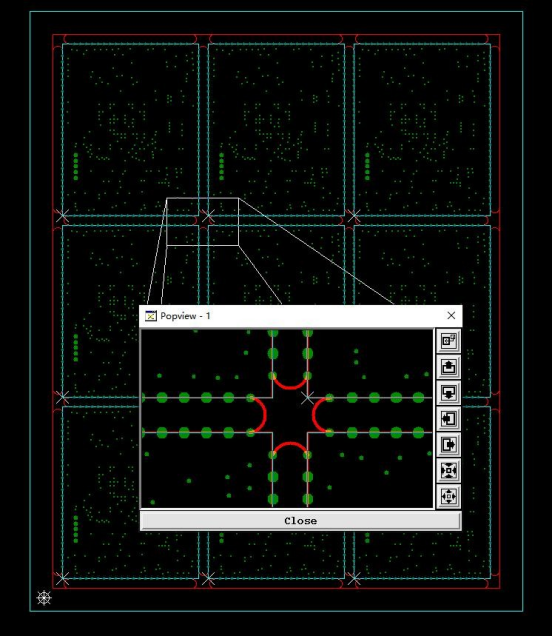
Stamp Hole Design
- Stamp hole sizes are typically between 0.3 – 0.8 mm (unless specified otherwise by the customer).
- The standard hole diameter is 0.5 mm, with one connection point designed every 70 mm.
- For other stamp hole diameters, ensure that the distance between holes and the number of stamp holes adhere to a minimum spacing of 0.5 mm.
- When designing, prioritize recessed configurations, where 2/3 of the stamp hole diameter is located within the finished board unit, ensuring proper spacing between holes, traces, and other components.
Stamp Hole Bridges + V-CUT
- When both stamp hole bridges and V-CUT designs are present at the same location, it is recommended to use only the V-CUT design.
- For locations with both bridges and V-CUTs (without stamp holes), the bridge width should be ≥ 3.0 mm.
Peripheral Half-Hole Boards with Stamp Holes
- For half-hole boards with solder spray, bridges with stamp holes should be drilled after the solder spray process to prevent the board from breaking during soldering.
- The size of the half-hole board bridges follows the standard design guidelines for stamp holes.
- If the bridge width after milling the half-hole is ≤ 1.0 mm, stamp holes are not needed.
- One stamp hole may be added for bridge widths between 1.0 mm and 1.5 mm.
Special Notes
- For customer-designed connection points, adhere to the above specifications wherever possible. If space allows, add one or two additional bridge groups.
- If customer-designed connection points do not meet the above guidelines, consult the customer and recommend redesigning the connection points according to these specifications.
- If the customer declines to modify the design, a process review should be conducted.

This approach ensures structural integrity, ease of processing, and reliability during PCB assembly.