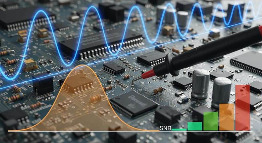
Back drilling, also known as controlled depth drilling, lets you take out unwanted via stubs from multilayer boards during PCB Manufacturing. This process helps make signal integrity better in high-speed circuits. If you know about back drilling, you can make better choices for quality and performance in your designs.
You can make your circuit boards better by learning how back drilling works and why it is important.
What is PCB Back Drilling?
Definition and Purpose
You may wonder what pcb back drilling means. This process removes extra copper from vias that run through multiple layers of a printed circuit board. When you use pcb back drilling, you target the unused part of a via, called a via stub. These stubs can cause problems for high-speed signals. By removing them, you help your board work better and faster.
You use pcb back drilling most often in multilayer boards. High-speed designs need clean signal paths. If you leave via stubs, you may see signal loss or unwanted reflections. You can avoid these issues by using pcb back drilling to clean up the vias. This step helps you get the best performance from your circuit.
Tip: If you design boards for data centers, servers, or telecom, you should consider pcb back drilling. It can make a big difference in signal quality.
Key Terms Explained
You will see some special words when you learn about pcb back drilling. Here is a quick guide to help you:
Term | What It Means |
|---|---|
Via | A small hole that connects different layers in a PCB. |
Via Stub | The unused part of a via that does not connect to any circuit on some layers. |
Back Drilling | The process of drilling out the via stub to improve signal integrity. |
Controlled Depth Drilling | A method to drill to a set depth without damaging other layers. |
How well a signal travels through a circuit without loss or distortion. |
You can use this table as a reference when you work with pcb back drilling. Knowing these terms will help you talk with engineers and manufacturers. You will also understand why this process matters for your projects.
Importance in PCB Manufacturing
Signal Integrity
You want your circuits to work fast and without errors. In pcb manufacturing, signal integrity means your signals travel cleanly from one point to another. If you leave via stubs in your board, signals can bounce back and cause problems. These problems can slow down your board or make it act in strange ways.
Back drilling helps you remove these stubs. When you use this process in pcb manufacturing, you make sure signals do not reflect or lose strength. This step is very important for high-speed boards. You can see better results in your data transfer and timing. Many engineers use back drilling for improving signal quality in their designs.
Note: Good signal integrity helps your devices last longer and work better.
Noise and Interference Reduction
Noise and interference can make your circuit board fail. In pcb manufacturing, you must keep these issues low. Via stubs can act like small antennas. They pick up unwanted signals and send them into your circuit. This can cause errors or even damage your board.
You can use back drilling to cut down on noise. When you remove the extra copper, you lower the chance of interference. This makes your pcb manufacturing process more reliable. You get cleaner signals and fewer problems during testing.
Less noise means your board works better in real-world conditions.
Lower interference helps you pass strict industry tests.
If you want strong and stable boards, focus on these steps in pcb manufacturing. You will see the benefits in every project.
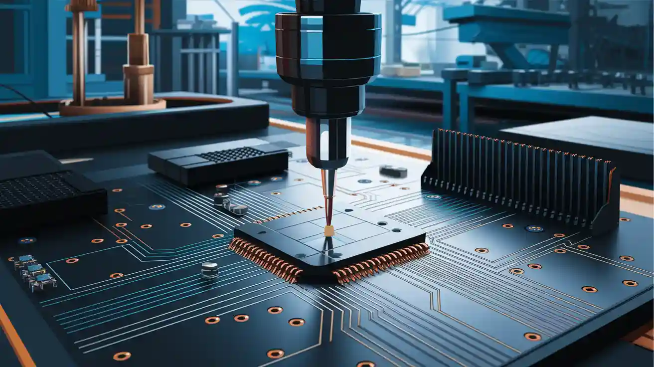
Back Drilling Process

Step-by-Step Overview
You need to follow a careful process when you use back drilling in PCB manufacturing. This process helps you remove via stubs and improve your board’s performance. Here is a simple step-by-step guide:
Identify the Target Vias
You start by finding the vias that need back drilling. These are usually the ones that create stubs in high-speed signal paths.Set Up the Drilling Machine
You program the drilling machine with the exact depth needed. This step is important because you want to reach the right layer without damaging others.Perform Controlled Depth Drilling
The machine drills into the via from the top or bottom side. It stops at the set depth, leaving the needed connections untouched. You only remove the unwanted stub.Inspect the Drilled Vias
You check the drilled holes to make sure the process worked. You look for clean holes and no damage to the layers.Clean and Finish the Board
You remove any debris from the drilling. The board is now ready for the next steps in manufacturing.
Tip: Always double-check your drilling depth before you start. Precision keeps your board safe and working well.
Tools and Depth Control
You need special tools for the back drilling process. The main tool is a CNC drilling machine. This machine can drill to a very exact depth. You also use sharp drill bits that match the size of your vias.
Depth control is the most important part of the process. You must set the drilling depth so you only remove via stubs. If you drill too deep, you can break the connections you need. If you drill too shallow, you leave part of the stub behind.
Here is a table to help you understand the main tools and their roles:
Tool | Purpose |
|---|---|
CNC Drilling Machine | Controls the drilling depth accurately |
Drill Bits | Cuts through copper and board material |
Depth Gauges | Checks the drilling depth during process |
You should always use machines that can handle controlled depth drilling. This keeps your layers safe and your signals strong.
Note: The back drilling process targets only the unwanted part of the via. You do not touch the layers that carry signals.
You can see how the right tools and careful depth control make the back drilling process safe and effective. You protect your board and improve its performance when you follow these steps.
Benefits and Challenges of Back-Drilled Vias
Performance Advantages
You can boost your PCB’s performance by using back drilling. This process removes unwanted via stubs, which helps your signals travel faster and cleaner. When you use back-drilled vias, you cut down on signal reflections and loss. Your high-speed circuits will work better because the signals do not bounce back or get distorted.
Here are some key benefits you get from back drilling:
Improved Signal Integrity: You keep your signals strong and clear by removing stubs.
Reduced Noise: Your board picks up less interference, so your data stays accurate.
Better Reliability: You lower the risk of errors in your circuits, which helps your devices last longer.
Higher Data Rates: You can design boards that support faster communication speeds.
Tip: If you want to meet strict industry standards, back-drilled vias can help you pass signal integrity tests.
Limitations and Considerations
You should also know the challenges of back drilling. This process needs special drilling machines and skilled operators. You must set the drilling depth with great care. If you drill too deep, you can damage the working layers of your PCB. If you drill too shallow, you leave part of the stub behind, which reduces the benefits.
Here is a table to help you see the main challenges:
Challenge | What You Need to Watch For |
|---|---|
Extra Cost | Back drilling adds to your manufacturing cost. |
You need precise drilling and careful planning. | |
Limited Use Cases | Not every board needs back-drilled vias. |
Risk of Damage | Incorrect drilling can harm your PCB layers. |
You should talk with your manufacturer before you add back drilling to your design. Make sure your project needs it and that you have the right tools for the job.
Note: Back drilling works best for multilayer, high-speed boards. Use it only when your design will benefit from it.
When to Use PCB Back Drilling
Ideal Applications
You should use PCB back drilling if your design needs fast signals. This process works best for boards with many layers and high-speed data. If you make devices for servers or routers, you may need back drilling. Many engineers use it in fast communication systems. It helps signals move quickly and without loss.
Back drilling is also good for test tools, medical gear, and aerospace electronics. These products need strong signals. If your board has lots of layers and uses fast signals, back drilling can help.
Here are some times when you should think about back drilling:
Multilayer PCBs with fast signals
Boards for data centers or telecom gear
Designs that must pass tough signal tests
Projects where noise and interference must stay low
Tip: If your board uses signals over 3 GHz, back drilling can help stop signal problems.
Best Practices
You can get the best results from back drilling by following some easy steps. First, plan your via structure when you design your board. Mark which vias need back drilling before sending files to the manufacturer. This step helps you avoid mistakes and saves time.
Use a table like this to track your back-drilled vias:
Via Location | Layer Start | Layer End | Needs Back Drilling? |
|---|---|---|---|
U1 | 2 | 8 | Yes |
J3 | 1 | 6 | No |
You should also talk with your PCB manufacturer. Tell them your goals and ask about drilling depth. Always check the finished board for clean holes and no damage.
Note: Good planning and talking with your manufacturer will help you get the most from back drilling.
You learned that PCB back drilling helps signals stay strong. It also makes your board work better. Use back drilling for boards with many layers or fast signals. This stops signals from getting weak or noisy.
Make a careful plan for your vias
Talk with your manufacturer often
Make sure the drilling depth is correct
Back drilling is a good way to fix signal problems in advanced PCB manufacturing.
FAQ
What is the main reason to use back drilling in PCBs?
You use back drilling to remove via stubs. This helps your signals move faster and stay clear. You get better signal integrity, especially in high-speed and multilayer boards.
Does back drilling increase the cost of PCB manufacturing?
Yes, back drilling adds extra steps and needs special machines. You may pay more for this process. You should use it only when your design needs better signal quality.
Can you use back drilling on every PCB?
No, you should not use back drilling on every board. You need it most for high-speed, multilayer designs. Simple boards or low-speed circuits do not need this process.
How do you know which vias need back drilling?
You check your design for vias that create stubs in high-speed paths. You mark these vias in your design files. Your manufacturer uses this information to drill only the needed spots.