You may ask if a printed circuit board can have an odd number of layers. The answer is yes, it can. But this kind of pcb is not seen often. Most makers pick even layers for better balance and trust. If you use an odd number of layers in your design, you will face special problems. Only a small part of the industry uses odd layers because these problems make it hard.
Key Takeaways
Odd-layer PCBs can be made, but they are not used much because they are harder to make.
Even-layer designs are chosen more often since they are more balanced, more stable, and cost less.
If you use odd layers, you might need special designs, like if you need the PCB to bend or fit in a small space.
Makers might need to do more work for odd-layer PCBs, which can make them take longer and cost more.
You should always talk to your PCB supplier to find out which layer setup is best for your project.
Odd-Layer PCB Basics
What Are Odd-Layer PCBs?
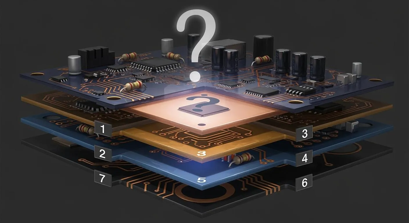
When you look at a printed circuit board, you usually see an even number of layers. An odd-layer PCB has a stack-up with an odd number of conductive layers, such as 3, 5, or 7. These layers include signal, power, and ground planes. Most multi-layer PCB designs use even numbers because they are easier to balance and manufacture. If you choose an odd number of layers, you may want to save space or meet a special design need. However, you will face extra challenges with this type of pcb multilayer board.
Note: Only a small part of the industry uses odd-layer PCBs. Most designers prefer even-layer multi-layer PCBs for better stability and lower cost.
PCB Layer Structure
The structure of a pcb with an odd number of layers is different from a standard multi-layer pcb. You need to pay close attention to how you arrange the layers. Here is what you should consider:
Balance copper distribution on each side of the board. This helps prevent bending and keeps the electrical properties stable.
Mirror the thickness of the dielectric material on both sides of the center. This keeps the board strong and helps with signal control.
Place power and ground planes so they mirror each other. This improves impedance matching and reduces noise.
Try to keep the layer count even when possible. Many designers add dummy layers to odd-layer boards to make them more balanced.
Odd-layer PCBs can bend more easily than even-layer boards. This happens because the lamination process creates different tensions in the core and outer layers. Warping can make manufacturing harder and increase costs. For this reason, you will often see designers change an odd-layer design into an even-layer one by adding extra layers. This helps create a balanced stack and makes the board more reliable.
A multi-layer pcb gives you more space for routing and better performance for high-speed signal designs. When you plan your pcb, think about the number of layers you need for your design. Most of the time, an even number of layers will give you the best results.
Odd-Layer PCB Manufacturing
Technical Feasibility
You might wonder if you can make a pcb with an odd number of layers. Yes, you can, but you will face more technical challenges than with even-layer boards. Most factories do not use odd-layer designs because they are harder to control and can affect the quality of your pcb multilayer board. Only about 8% of all pcbs use an odd number of layers. This low number shows how rare and difficult these boards are to produce.
When you build a multi-layer pcb, you need to keep the layers balanced. If you do not, your board can bend or warp. Odd-layer PCBs make this balance harder to achieve. For example, a four-layer board can keep its shape well, with warpage controlled at 0.7%. A three-layer board can bend more, which can hurt the quality of your finished product. This bending can cause problems when you add chips or other parts to your pcb.
Here is a table that shows the main technical challenges you will face when making odd-layer PCBs:
Challenge | Description |
|---|---|
Warping | Etching away copper from one side causes warping. You need a balanced setup of pre-peg and base layers. |
Copper Plating | Uneven weight from the odd-layer design can lead to over-plating or under-plating during the process. |
Bending | Laminating tensions during cooling can cause bending, especially with increased thickness of the pcb. |
Note: If you do not control these issues, your pcb may not work as planned. You may also see higher costs and more waste during production.
Stacked Core Process
To make odd-layer PCBs, you need to use a non-standard stacked core process. This process is different from what you use for even-layer boards. You must add extra steps to the normal core structure. These extra steps can slow down production and make it harder to keep your board free from defects.
Here are some ways the stacked core process for odd-layer pcbs is different:
You must add a special lamination core bonding process on top of the normal core structure. This step is not needed for even-layer boards.
Factories often add foil to the outside of the core structure. This step lowers production speed and can make the process less efficient.
The outer core needs extra processing before you can laminate and bond the layers. This extra handling increases the risk of scratches and etching mistakes on the outer layer.
Odd-layer designs need unique production steps. These steps can raise labor costs and increase the chance of errors. You may need to try several times to get the process right.
When you design a pcb with an odd number of layers, you must plan for these extra steps. You also need to think about the risks. Most designers choose even-layer multi-layer pcbs because they are easier to make and more reliable. If you need a special design with odd layers, talk to your manufacturer first. They can help you decide if the extra work and cost are worth it for your project.
Odd-Layer PCB Pros and Cons
Advantages
Sometimes, engineers pick odd-layer pcbs for special reasons. These boards can help in certain cases. Here are some reasons to use odd-layer pcbs:
You can get shielding on both sides in flex areas. This helps keep signal paths safe.
Odd-layer designs can control stripline impedance better. This is important for RF and EMI work.
Fewer conductive layers in flex areas make the pcb thinner. This also makes it more flexible.
More flexibility means the board bends better. This helps in devices that need to fold or bend.
You might save money by using fewer flex layers.
These good points make odd-layer pcbs useful for some multi-layer designs. They work well when you need both flexibility and strong signals.
Disadvantages
Odd-layer pcbs also have some problems. When making these boards, one copper foil does not have a pair. This adds extra steps and causes uneven stress in the pcb multilayer board. Because of this, costs go up and defects can happen more often. Multi-layer pcbs with even stacks stop warping during heat cycles. If one side has more copper or resin, the board can bend after soldering. Even layers keep both sides even and steady. Odd-layer boards have trouble staying balanced. This can hurt how well they work and how long they last. For most multi-layer pcb jobs, even layers are safer and cost less.
Multi-Layer PCB Design and Industry Practice
Why Even Layers Are Preferred
When you design a multi-layer pcb, you want your board to stay flat and strong. Most manufacturers choose even layers for several reasons:
Even layers keep the pcb balanced. This balance helps prevent warping or bending during manufacturing.
The process for making even-layer pcbs is simple and efficient. Factories set up their machines to work best with even numbers of layers.
Adding layers in pairs saves time and materials. Odd-layer pcbs need extra steps, which makes them more expensive.
You will see that even-layer boards give you better results for most projects. They help you avoid problems with signal quality and board strength. If you want a reliable pcb, you should pick an even number of layers.
Multi-Layer PCB Design Challenges
Odd-layer pcbs bring extra challenges to your design. You may face problems with the way the board bends or how the weight spreads across the layers. Here is a table that shows some of the main issues:
Challenge | Description |
|---|---|
Warpage | Odd layers cause stress that can make the pcb warp, especially after soldering. |
Weight Distribution | Uneven weight can lead to problems with plating, making the board less reliable. |
Design Preference | Most experts suggest using even layers to avoid these issues. |
When you use odd layers, you make the design process harder. You may need to spend more money and time to fix problems. Many designers choose even layers because they want a stable and cost-effective multi-layer pcb. Even layers help you keep your signal paths clear and your board strong. If you want to avoid trouble, stick with even-layer multi-layer pcbs for your next design.
When to Use Odd-Layer PCBs
Special Design Requirements
You may find that most projects do not need odd-layer PCBs. Sometimes, though, your design will have unique needs. You might want to make your pcb thinner or lighter. Odd layers can help you reach a specific thickness that even layers cannot provide. You may also need to fit your board into a tight space. In these cases, you can use an odd number of layers to save room. Some engineers use odd-layer boards to improve signal control in special circuits. For example, you may want to keep certain signals away from others. Odd layers can help you separate these paths.
You should remember that odd-layer PCBs often need extra planning. You must talk with your manufacturer before you start. They can help you decide if odd layers will work for your project. If you want to try a new multi-layer pcb design, you should check if odd layers will give you the results you need.
Tip: Always ask your pcb supplier about the best way to build your board. They know which stack-up will work best for your design.
Niche Applications
You will see odd-layer PCBs in a few special industries. These boards help when you need a small, light, or flexible product. Here are some places where odd-layer PCBs are common:
Wearable devices like smart watches and fitness trackers use odd layers to keep the pcb thin and flexible.
Medical implants need boards that fit the shape of the body. Odd layers help the pcb bend and stay strong.
Automotive sensors often go in tight spots. Odd-layer PCBs make it easier to connect parts in small spaces.
Aerospace interconnects must be light. Odd layers help reduce weight in these sensitive systems.
You may not use odd-layer PCBs every day. Still, they can solve problems in special cases. If your project needs a custom shape or must fit in a small space, you should think about using odd layers. Always weigh the benefits against the extra cost and work. Most of the time, even layers will give you a better result. Odd layers work best when your design has a clear need for them.
You can make a circuit board with an odd number of layers. But most experts say you should use even-layer stack-ups. Even-layer PCBs are more balanced and cost less. They also work better for electricity than odd-layer designs. The table below shows the main differences:
Aspect | Even-Layer PCBs | Odd-Layer PCBs |
|---|---|---|
Manufacturing Cost | Lower | Higher |
Risk of Warping | Lower | Higher |
Electrical Performance | Improved | Decreased |
Processing Efficiency | Higher | Lower |
If you do not have a special reason, pick a double-layer or single-layer pcb. Or use signal layers that are balanced. Always talk to your manufacturer before you change from a single-layer pcb design.
FAQ
Can you use an odd number of layers in a PCB design?
Yes, you can use an odd number of layers in a pcb design. You may face more challenges with manufacturing and reliability. Most engineers choose even numbers for better results.
Why do most printed circuit boards have even layers?
You see even layers in most printed circuit boards because they give better balance and strength. This choice helps prevent warping and keeps the board flat during use.
Do odd-layer PCBs cost more to make?
You will pay more for odd-layer pcbs. The process takes extra steps and time. Manufacturers need special handling, which increases the price.
Are odd-layer PCBs less reliable?
Odd-layer pcbs can bend or warp more easily. You may see more defects and lower performance. Even-layer boards usually last longer and work better.
When should you choose an odd-layer PCB?
You should pick an odd-layer pcb only for special needs. For example, you may need a thinner board or a unique signal path. Always talk to your manufacturer first.